 ALLPCB


Introduction
Polytetrafluoroethylene, or PTFE, represents a premium substrate material in printed circuit board fabrication, particularly for demanding environments like medical devices. Electrical engineers designing for medical applications often select PTFE PCBs due to their exceptional electrical stability and resistance to environmental stressors. These boards support high-frequency signal integrity essential in imaging systems and implantable electronics. In medical contexts, reliability directly impacts patient safety, making material choices critical. PTFE PCBs address these needs through inherent properties that maintain performance over extended lifecycles. This article explores their role in PTFE PCB medical applications, focusing on biocompatibility and regulatory alignment.
What Are PTFE PCBs and Why Do They Matter in Medical Devices?
PTFE PCBs utilize polytetrafluoroethylene as the core laminate, a fluoropolymer known for its low dielectric constant and minimal dissipation factor. Unlike standard FR-4 materials, PTFE offers superior signal propagation at microwave frequencies, reducing attenuation in sensitive circuits. Factory processes for PTFE demand specialized handling to prevent contamination and ensure uniform lamination. In medical devices, these boards power applications from diagnostic ultrasound to wireless telemetry in pacemakers. Their stability under thermal cycling and chemical exposure aligns with high-reliability requirements.
The relevance stems from medical electronics' need for uninterrupted operation in sterile, humid, or bodily fluid-exposed settings. PTFE's chemical inertness prevents degradation that could compromise circuit function. Engineers prioritize these boards for devices requiring precise RF performance, such as MRI subsystems. Moreover, PTFE PCB biocompatibility supports integration into patient-contact systems without eliciting adverse reactions. Factory-driven insights reveal that selecting PTFE elevates device longevity, aligning with risk management protocols in healthcare.
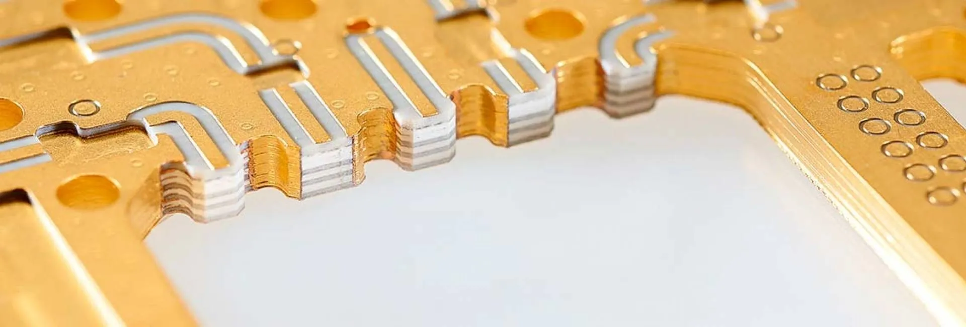
Key Technical Properties of PTFE PCBs for Medical Reliability
PTFE exhibits a dielectric constant around 2.1, stable across broad frequency ranges, which minimizes impedance mismatches in high-speed traces. This property proves vital in medical imaging where signal fidelity affects diagnostic accuracy. Low loss tangent further reduces heat generation during operation, preserving component integrity. Thermal expansion coefficients closely match copper, mitigating warpage during soldering or autoclave sterilization. These characteristics ensure dimensional stability per manufacturing tolerances.
Chemical resistance defines PTFE's edge in medical settings, resisting solvents, bodily fluids, and disinfectants without delamination. Moisture absorption remains below 0.02 percent, preventing ionic migration that leads to failures. In high-reliability fabrication, adherence to IPC-6012 qualification specifications verifies these traits through thermal shock and reliability testing. Biocompatibility testing, guided by ISO 10993, confirms no cytotoxicity or sensitization from PTFE extracts. Electrical engineers leverage these for multilayer stacks in compact implants.
Mechanical robustness includes high peel strength and low modulus, accommodating flexure in wearable diagnostics. Factory lamination uses controlled pressure to embed reinforcements like glass fabric, enhancing rigidity. Performance in elevated temperatures up to 260 degrees Celsius supports lead-free assembly processes. Overall, these mechanisms underpin PTFE PCB medical applications' dependability.
Biocompatibility and Regulatory Considerations for PTFE PCBs
PTFE's inert nature positions it as biocompatible, with no leaching of harmful substances in physiological environments. Regulatory bodies recognize fluoropolymers like PTFE for safe use in devices from catheters to implants. PTFE PCB biocompatibility extends to electronics where boards may contact tissues indirectly through enclosures. FDA evaluations affirm no patient health risks from such materials in approved devices. Engineers must document material compliance during device submissions.
Manufacturing integrates biocompatibility validation early, including extractables analysis. Standards like ISO 10993 outline tests for irritation, genotoxicity, and implantation. For PCBs, surface finishes and soldermasks must also pass these. Factory protocols ensure traceability from resin to finished board. This holistic approach secures PTFE PCB FDA approval pathways for Class II and III devices.
Best Practices in Designing and Fabricating PTFE PCBs for Medical Use
Design begins with stackup optimization, placing high-speed signals on inner PTFE layers to shield from EMI. Controlled impedance modeling accounts for PTFE's low Dk variability. Via structures employ blind or buried types to minimize stubs affecting RF paths. Engineers specify enamel wire bonding over standard plating for better adhesion on PTFE's smooth surface. Sequential lamination builds complex multilayers without voids.
Fabrication demands cleanroom conditions to avoid filler migration during pressing. Prepreg selection matches resin content for flow control, preventing resin starvation. Bake-out removes volatiles prior to lamination, per IPC-A-610 acceptability criteria for high-reliability assemblies. Post-process inspections include cross-sectioning for glass alignment and thermal cycling simulations. Electrical testing verifies continuity and insulation resistance under humidity.
Assembly challenges include higher soldering temperatures; nitrogen reflow atmospheres reduce oxidation. Component placement avoids stress on PTFE's softer core. Final conformal coatings enhance moisture barriers. These practices ensure PCBs meet Class 3 performance in medical validation.
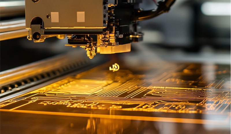
Manufacturing Insights and Quality Control for Long-Term Performance
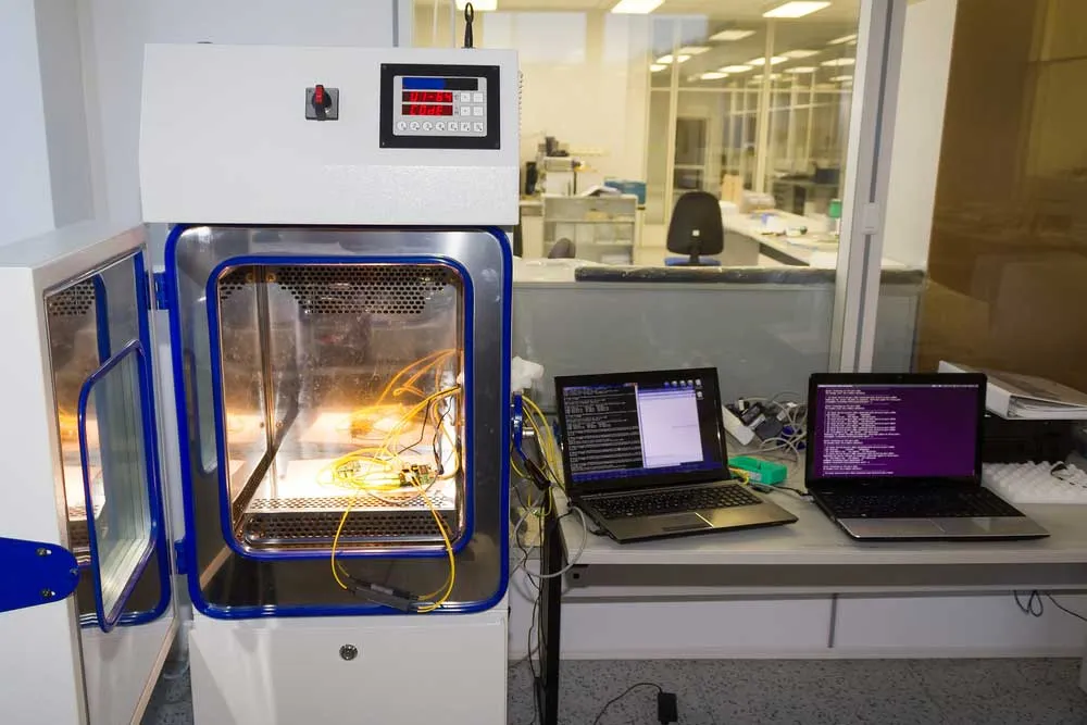
Factory experience highlights PTFE's sensitivity to drill smear, necessitating plasma cleaning for reliable plating. Aspect ratios stay conservative to maintain hole wall integrity. Reliability screening includes HAST and thermal shock per industry protocols. Dimensional checks post-bake confirm flatness for automated assembly. Traceability logs every lot, supporting audit trails.
In medical production, yield optimization focuses on uniform curing to avoid CTE mismatches. Reinforced PTFE variants balance pure resin's benefits with mechanical strength. Ion chromatography detects contaminants early. These steps align with factory-driven quality for sustained field performance.
Conclusion
PTFE PCBs deliver unmatched reliability and performance in medical devices through superior electrical, thermal, and chemical properties. Their role in high-frequency PTFE PCB medical applications underscores biocompatibility and stability needs. Adhering to standards like IPC-6012 and ISO 10993 ensures compliance and safety. Electrical engineers benefit from factory insights into design and fabrication best practices. Selecting PTFE elevates device outcomes, fostering innovation in healthcare electronics.
FAQs
Q1: What makes PTFE PCBs suitable for PTFE PCB medical applications?
A1: PTFE PCBs excel in medical applications due to low dielectric loss and high thermal stability, supporting RF signals in imaging and telemetry. Their chemical resistance withstands sterilization, while low moisture uptake prevents failures. Factory processes ensure Class 3 compliance, enhancing device longevity. Biocompatibility aligns with patient safety requirements.
Q2: How does PTFE PCB biocompatibility impact medical device design?
A2: PTFE PCB biocompatibility minimizes risks in tissue-proximate electronics, passing ISO 10993 cytotoxicity tests. Inertness prevents inflammation, ideal for implants. Engineers select it for non-reactive performance in bodily fluids. Regulatory history supports seamless integration into FDA pathways.
Q3: What role does PTFE PCB FDA approval play in high-reliability medical PCBs?
A3: PTFE materials in PCBs contribute to FDA approval by demonstrating no health risks in devices like pacemakers. Evaluations confirm safe fluoropolymer use without restrictions. Compliance involves full device testing, including PCB reliability data. This assures performance in critical applications.
Q4: Why choose PTFE over FR-4 for medical high-frequency circuits?
A4: PTFE outperforms FR-4 with lower Dk and Df for better signal integrity at GHz frequencies. It handles extreme temperatures and chemicals better, vital for sterilization. Factory lamination yields stable boards per IPC standards. This choice boosts reliability in demanding medical environments.
References
IPC-6012 — Qualification and Performance Specification for Rigid Printed Boards. IPC.
IPC-A-610 — Acceptability of Electronic Assemblies. IPC.
ISO 10993 — Biological evaluation of medical devices. ISO.





