 ALLPCB


Introduction
In PCB design, power planes represent a fundamental element that ensures efficient power distribution across multilayer boards. These dedicated copper layers carry supply voltages to various components, minimizing voltage drops and maintaining signal integrity. Electric engineers rely on power planes to handle high current demands in complex circuits, where traditional traces fall short. By providing a low-impedance path, power planes reduce electromagnetic interference and support faster switching speeds in modern electronics. This article explores the role of power planes, their integration with vias and components for strong connections, and best practices in PCB design. Understanding these aspects helps engineers optimize performance and reliability in demanding applications.
Power planes have evolved with the shift to multilayer PCBs, becoming essential for high-density designs. They differ from signal layers by focusing solely on power delivery rather than data transmission. In PCB design workflows, allocating layers for power and ground planes early prevents layout issues later. Engineers must consider stackup configuration to pair power planes with adjacent ground planes for optimal capacitance. This setup forms a distributed decoupling network, crucial for noise suppression.
What Is a Power Plane?
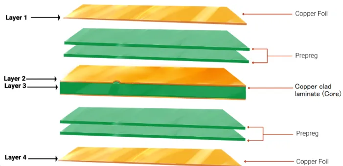
A power plane consists of a continuous or nearly continuous sheet of copper on one or more layers of a PCB, dedicated to distributing DC power or specific voltage rails. Unlike traces, which route signals point-to-point, power planes offer uniform voltage across the board due to their broad area. In PCB design, engineers define power planes during the layer stackup phase, typically placing them in inner layers for shielding. Solid power planes cover the entire layer except for clearances around other nets, while split planes serve multiple voltages with anti-pad cutouts.
The thickness of power planes, often 1 or 2 ounces per square foot of copper, determines their current-carrying capacity. Thicker planes handle higher currents with less resistance, but manufacturing constraints limit options. Hatched or meshed power planes reduce weight and material cost in some applications, though they introduce higher inductance. Engineers select plane types based on thermal and electrical needs, ensuring compatibility with components.
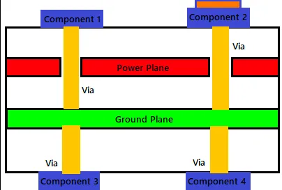
Power planes connect to components through vias, forming strong connections that transfer current reliably. Vias act as vertical conduits between layers, linking the plane to surface-mount pads or through-hole pins. In PCB design, proper via placement prevents hotspots and ensures even power flow. Without adequate via stitching, planes can exhibit discontinuities that degrade performance.
Why Power Planes Matter in PCB Design
Power planes deliver several critical benefits in PCB design, starting with low-impedance power distribution. This characteristic keeps voltage stable under dynamic loads from switching components like processors and FPGAs. Traditional trace-based distribution suffers from higher resistance and inductance, leading to ground bounce and voltage sag. Power planes mitigate these by spreading current evenly, supporting high-frequency operation.
Another key advantage lies in electromagnetic compatibility. Adjacent ground planes and power planes create a controlled impedance environment for signals routed between them. This stripline configuration reduces crosstalk and radiation, vital for compliance in dense boards. In PCB design, engineers prioritize power plane placement to shield sensitive analog sections from digital noise.
Thermal management improves with power planes, as their large area dissipates heat effectively. Current flow generates I squared R losses, but broad planes spread this heat, avoiding localized hotspots. Components connected via vias benefit from this, maintaining junction temperatures within limits. Power planes also simplify routing by freeing signal layers for traces.
For strong connections, power planes enable multiple vias per component, distributing current and reducing stress on individual joints. This redundancy enhances reliability under vibration or thermal cycling. In high-power applications, such as power supplies or motor drives, power planes prevent failures from electromigration.
Technical Principles of Power Planes
The core principle of power planes revolves around minimizing DC resistance and AC inductance. Resistance follows the formula R equals rho times length over area, where the large area of planes yields very low values. For AC performance, inductance depends on loop area between power and return paths; tight coupling with ground planes reduces it. In PCB design, engineers calculate plane impedance using field solvers to verify margins.
Vias play a pivotal role in coupling power planes to components, creating strong connections through plated barrels. Through vias penetrate the plane, while blind or buried vias connect specific layers. Stitching vias, placed densely around component footprints, tie split planes and provide return paths for high-frequency currents. Poor via density leads to impedance discontinuities, exciting resonances.
Power integrity analysis reveals how planes handle simultaneous switching noise. Decoupling capacitors bridge power and ground planes near components, shunting high-frequency noise. The plane pair forms a low-pass filter, with effective capacitance proportional to area and dielectric constant. Engineers model this in simulations to predict PDN impedance targets below 1 ohm up to GHz frequencies.
Clearances and splits in power planes prevent shorting between voltage domains. Anti-pads isolate sections, but sharp corners can concentrate fields, risking arcing. Rounded splits and overlapping clearances maintain field uniformity. According to IPC-2221B, design rules for clearances ensure safe spacing based on voltage levels.
Thermal expansion affects power planes, as copper coefficients differ from dielectrics. This mismatch causes warpage in multilayer boards, stressing via connections. Symmetric stackups with balanced copper distribution mitigate this. Vias must withstand shear forces, with plating thickness per IPC-6012E specifications.
Best Practices for Power Planes in PCB Design
Start power plane implementation by dedicating full layers early in PCB design. Pair each power plane with a ground plane to maximize coupling and minimize loop inductance. Avoid routing signals over splits to prevent field distortion. Use 2-ounce copper for high-current planes, verifying current capacity against thermal rise limits.
Via placement demands density near high-current components. For strong connections, use via arrays under power pins, with 0.3 mm pitch minimums. Stitch plane edges every 1/20 wavelength of highest frequency to contain fields. Fanout vias from BGA balls directly to planes, minimizing stubs.
Decoupling strategy integrates capacitors between planes at IC power pins. Place 0.1 uF ceramics within 1 mm, supplemented by bulk caps for low frequencies. In PCB design, route cap vias short to planes, avoiding traces. This forms a multi-stage filter for broadband noise suppression.
Split planes require careful partitioning. Extend splits beyond component boundaries by 10 mils for margin. Connect islands with necked-down sections if same voltage, but isolate different rails completely. Simulate DC drops to ensure less than 5% variation.
Power plane voids for components need oversized anti-pads. Maintain 10 mil clearance minimums, filleting corners. For high-voltage, follow IPC-2221B creepage rules. Test prototypes with TDR for impedance continuity.
Manufacturing considers plane tenting and etching. Specify soldermask over planes for protection, but open windows at vias. Etch tolerances affect thin splits, so widen critical features. Post-etch inspection per IPC-A-600K verifies continuity.
Common Challenges and Troubleshooting
One challenge in power planes is DC voltage droop from uneven current distribution. High-di pins draw more current, starving distant components. Solution: add decoupling and verify with IR drop analysis. Vias in high-current paths need larger barrels to avoid necking.
Resonances from unstitched planes cause PDN peaks. Dense stitching or embedded caps resolve this. EMI leakage occurs at plane edges; wrap with ground stitching.
Component connections fail from via cracking under thermal stress. Use filled vias or larger pads. Simulate thermomechanical stress.
Conclusion
Power planes stand as a cornerstone in PCB design, enabling low-impedance distribution, noise control, and reliable component connections. Integrating vias thoughtfully ensures strong connections, while adherence to principles like plane pairing boosts performance. Electric engineers benefit from structured approaches, from stackup planning to simulation. Mastering these elements leads to robust, high-speed boards.
FAQs
Q1: What role do power planes play in PCB design?
A1: Power planes in PCB design provide low-impedance paths for voltage distribution to components. They reduce voltage drops and support high-current loads better than traces. Paired with ground planes, they form effective decoupling. Vias connect them strongly to components, ensuring stable operation. Following guidelines like IPC-2221B optimizes layouts.
Q2: How do vias ensure strong connections to power planes?
A2: Vias in PCB design link components directly to power planes, distributing current evenly. Stitching vias around footprints prevent discontinuities and provide return paths. Arrays of vias handle high currents without hotspots. Proper sizing and plating maintain integrity under stress. This setup enhances reliability in multilayer boards.
Q3: Why are power planes essential for components in PCB design?
A3: Power planes deliver consistent voltage to components, minimizing noise and droop. In PCB design, they simplify routing and improve thermal dissipation. Strong connections via vias reduce joint stress. They support dense layouts with multiple rails. Engineers prioritize them for signal integrity.
Q4: What best practices apply to power planes and vias?
A4: Dedicate layers for power planes adjacent to grounds in PCB design. Place stitching vias densely for strong connections. Use decoupling caps near components. Simulate impedance and drops. Maintain clearances per standards to avoid shorts.
References
IPC-2221B — Generic Standard on Printed Board Design. IPC, 2003
IPC-6012E — Qualification and Performance Specification for Rigid Printed Boards. IPC, 2017
IPC-A-600K — Acceptability of Printed Boards. IPC, 2020


