 ALLPCB


Designing multi-layer PCBs for complex systems comes with unique hurdles, especially when it comes to power integrity. If you're an engineer working on intricate PCB layouts, you might be facing issues like voltage drops, noise, and signal distortions caused by via inductance and plane resonance. So, how can you tackle these power integrity challenges in multi-layer PCB designs? The key lies in understanding the root causes and applying targeted solutions such as proper layer stacking, decoupling capacitor placement, and optimized via design to ensure stable power delivery and minimal interference.
In this blog, we'll dive deep into the specific power integrity challenges of multi-layer PCBs, focusing on complex designs. We'll explore practical solutions to common issues like via inductance and plane resonance, providing actionable tips to help you create reliable and high-performing boards. Whether you're dealing with high-speed signals or dense layouts, this guide will equip you with the knowledge to overcome PCB design challenges.
What is Power Integrity in Multi-Layer PCB Design?
Power integrity refers to the ability of a PCB to deliver stable and clean power to all components on the board. In multi-layer PCBs, where multiple layers are stacked to accommodate complex circuits, maintaining power integrity becomes even more critical. These designs often support high-speed digital circuits, analog components, and mixed-signal systems, all of which demand consistent voltage levels and minimal noise.
Without proper power integrity, you might encounter problems like voltage fluctuations, electromagnetic interference (EMI), and signal degradation. These issues can lead to system failures or reduced performance, especially in applications like telecommunications, automotive electronics, and medical devices. Understanding power integrity is the first step to addressing the challenges in complex PCB design.
Key Power Integrity Challenges in Multi-Layer PCBs
Multi-layer PCBs offer advantages like compact size and enhanced functionality, but they also introduce specific challenges for power integrity. Let's break down the most common issues engineers face when working on complex designs.
1. Via Inductance and Its Impact on Power Delivery
Vias are essential in multi-layer PCBs for connecting different layers, but they introduce parasitic inductance. This via inductance can impede the flow of current, especially in high-frequency designs, leading to voltage drops and noise in the power delivery network (PDN). For instance, in a high-speed design operating at 1 GHz, even a small inductance of 1 nH can cause significant impedance, disrupting power integrity.
The problem worsens when multiple vias are used in a dense layout, as the cumulative inductance can create bottlenecks in power distribution. This often results in inadequate power supply to critical components, causing performance issues.
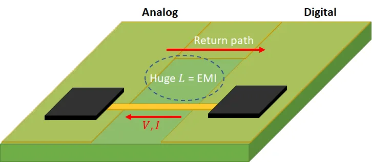
2. Plane Resonance and Noise Coupling
In multi-layer PCBs, power and ground planes are used to distribute voltage and provide a return path for signals. However, these planes can act as resonant structures at certain frequencies, leading to plane resonance. When the frequency of the system matches the resonant frequency of the planes—often in the range of 100 MHz to 1 GHz—voltage fluctuations and noise coupling occur.
This resonance can amplify noise, which then interferes with sensitive signals, especially in high-speed designs. For complex PCB designs with mixed analog and digital signals, plane resonance can be a major source of crosstalk and EMI.
3. High-Density Layouts and Limited Space
Complex PCB designs often require high-density layouts to fit numerous components into a small footprint. While multi-layer PCBs help by stacking circuits vertically, this density makes it harder to allocate space for power distribution networks. Limited space for decoupling capacitors, wide power traces, or dedicated ground planes can compromise power integrity, leading to uneven power distribution.
4. High-Speed Signal Interference
High-speed signals, common in modern electronics, demand low-noise power supplies. In multi-layer PCBs, the close proximity of signal traces to power planes can lead to interference if the PDN is not well-designed. For example, a signal switching at 2.5 Gbps can induce noise in the power plane, affecting other components and degrading overall system performance.
Solutions for Power Integrity Challenges in Complex PCB Designs
Addressing power integrity challenges in multi-layer PCBs requires a combination of careful planning, simulation, and design optimization. Below are proven solutions tailored to the issues of via inductance, plane resonance, and other PCB design challenges.
1. Optimize Via Design to Minimize Inductance
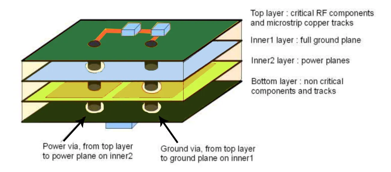
To reduce via inductance, focus on minimizing the length and loop area of vias in your design. Shorter vias have lower inductance, so place components and power planes on adjacent layers whenever possible. Additionally, using multiple vias in parallel for power and ground connections can distribute current more evenly and reduce the effective inductance. For example, using four vias instead of one can cut inductance by up to 75%.
Another approach is to use microvias or buried vias, which are smaller and create less inductance compared to through-hole vias. These are particularly useful in high-density, complex PCB designs where space is limited.
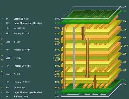
2. Mitigate Plane Resonance with Proper Stackup Design
Plane resonance can be minimized by carefully designing the layer stackup of your multi-layer PCB. Place power and ground planes close to each other to increase capacitance between them, which helps dampen resonance. A typical spacing of 5 to 10 mils between planes can significantly reduce resonant effects at high frequencies.
Additionally, avoid large, uninterrupted power planes that can act as resonant cavities. Instead, split planes into smaller sections for different voltage domains while ensuring each section has adequate decoupling. Simulation tools can help identify resonant frequencies during the design phase, allowing you to adjust the stackup before fabrication.
3. Use Decoupling Capacitors Strategically
Decoupling capacitors are critical for maintaining power integrity by filtering out noise and stabilizing voltage levels. Place these capacitors as close as possible to the power pins of ICs to minimize the loop inductance. A good rule of thumb is to use a range of capacitor values—such as 0.1 μF, 1 μF, and 10 μF—to cover different frequency ranges of noise.
In high-density layouts, consider using embedded capacitors within the PCB layers if surface space is limited. These can provide low-inductance decoupling directly between power and ground planes, improving power integrity in complex designs.
4. Implement Robust Grounding Techniques
A solid grounding strategy is essential for reducing noise and interference in multi-layer PCBs. Dedicate entire layers to ground planes to provide a low-impedance return path for signals. Ensure that ground vias are placed near signal vias to minimize loop areas and reduce EMI.
For mixed-signal designs, separate analog and digital grounds to prevent noise coupling, connecting them at a single point to avoid ground loops. This approach helps maintain power integrity across different sections of the board.
5. Simulate and Test Power Distribution Networks
Before finalizing your design, use simulation tools to analyze the power distribution network. These tools can model impedance profiles, identify potential resonance issues, and predict voltage drops across the board. For instance, a target impedance of 0.1 ohms or less is often recommended for high-speed designs to ensure minimal voltage ripple.
After fabrication, perform physical testing with oscilloscopes and network analyzers to validate power integrity. Measure voltage noise levels and compare them against design specifications to confirm that your solutions are effective.
Best Practices for Complex PCB Design with Power Integrity in Mind
Beyond specific solutions, adopting best practices during the design phase can prevent power integrity issues from arising in multi-layer PCBs. Here are some tips to keep in mind for complex designs:
- Prioritize Layer Planning: Plan your layer stackup early to allocate space for power and ground planes, ensuring balanced distribution across the board.
- Minimize Signal-Powe


