ALLPCB


Overview of the portable ultrasound power system
The internal power architecture of a portable ultrasound system is relatively complex. External adapter and battery supplies must pass through DC/DC conversion to generate the voltages required by the system. To minimize wasted power and improve battery efficiency, the mainboard, ultrasound control board, LCD, and keyboard are powered by switching power supplies.
Figure 1 shows the block diagram for the portable ultrasound power system. The system accepts two input voltages: an external adapter at 18 V and a battery at 14.4 V. The design implements a seamless hot-swap between these sources so that switching does not interrupt system operation. Required outputs are ±12 V, 5 V, 3.3 V, and ±48 V with the following ratings: +12 V/2.5 A, -12 V/0.5 A, +5 V/4 A, +3.3 V/3 A, +48 V/80 mA, -48 V/80 mA. A single-key power on/off function is implemented: if no external power is present, pressing the power key turns the device on; if external power is present, pressing the power key sends a shutdown signal to the control panel. The host PC can also issue a software shutdown (ATX power-off command). The power output connector uses a standard computer ATX interface.
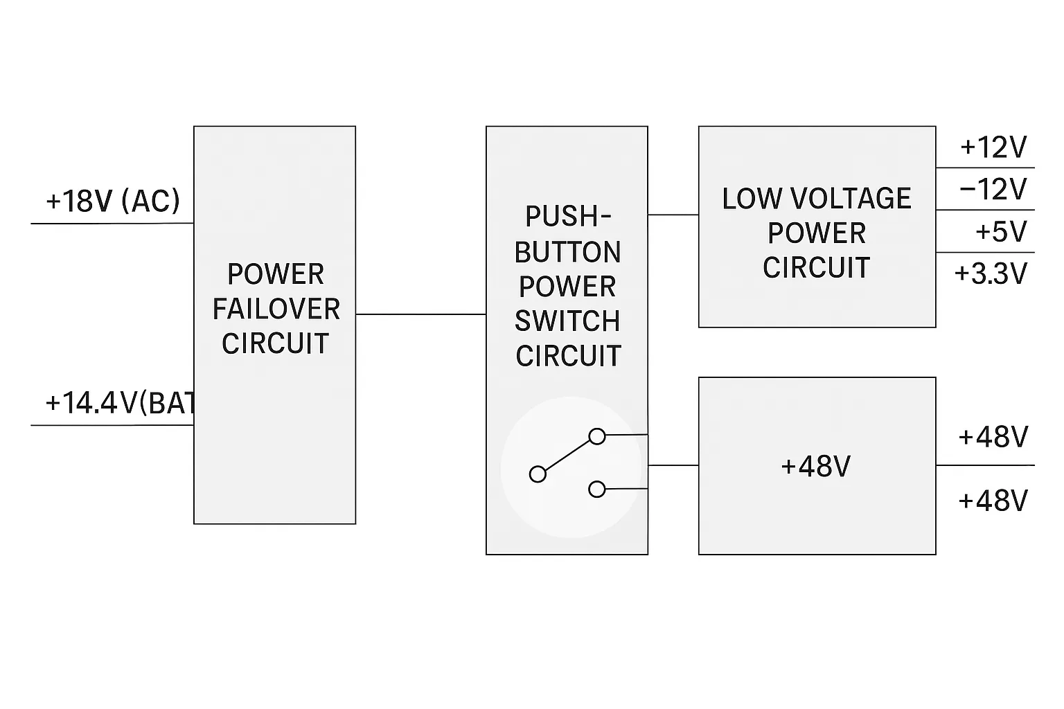
Figure 1 Portable ultrasound power supply block diagram
Power source switching circuit
The power switching circuit for the portable ultrasound is shown in Figure 2. When an external adapter is connected, the adapter provides 18 V which is rectified by diodes VD100 and VD101, then fed through R100 and R107 as a divider to pin 3 (noninverting input) of comparator N100A (LM193). The battery input of 14.4 V is divided by R101 and R108 and fed to pin 2 (inverting input) of N100A. Because the voltage at pin 3 is higher than pin 2, N100A outputs a high level on pin 1, turning transistor V100 on, holding V101 off, and keeping MOSFET V105 off. As a result, POWER_IN+ receives the external adapter voltage of 18 V.
If the external adapter is absent or AC power fails during operation, the voltage at pin 3 of N100A falls below pin 2. N100A then outputs a low level on pin 1, turning V100 off, turning V101 on, and turning MOSFET V105 on. The battery voltage is passed through V105 source-drain to POWER_IN+, providing 14.4 V and achieving the hot-swap between the two sources. Diodes VD102 and VD103 isolate the external adapter and battery supplies.
Single-key touch power on/off circuit
The single-key touch power circuit is shown in Figure 3. POWER_IN+ from the external adapter or battery is routed to MOSFET Q100 for power delivery, and via R104 and VD104 to one side of the touch pushbutton POWER-KEY2. The other side of POWER-KEY2 is grounded. When POWER-KEY2 is pressed, transistor N106 base is clamped low, N106 conducts, which in turn drives N102 to conduct and Q100 to turn on. POWER_IN+ then passes through Q100 source-drain to produce POWER+, which supplies the high- and low-voltage circuits and powers the system.
On power-up, POWER+ is used through a 6 V zener diode to turn on transistor N104. N104 pulls its collector low, which maintains N106 conduction and latches the power-on state.
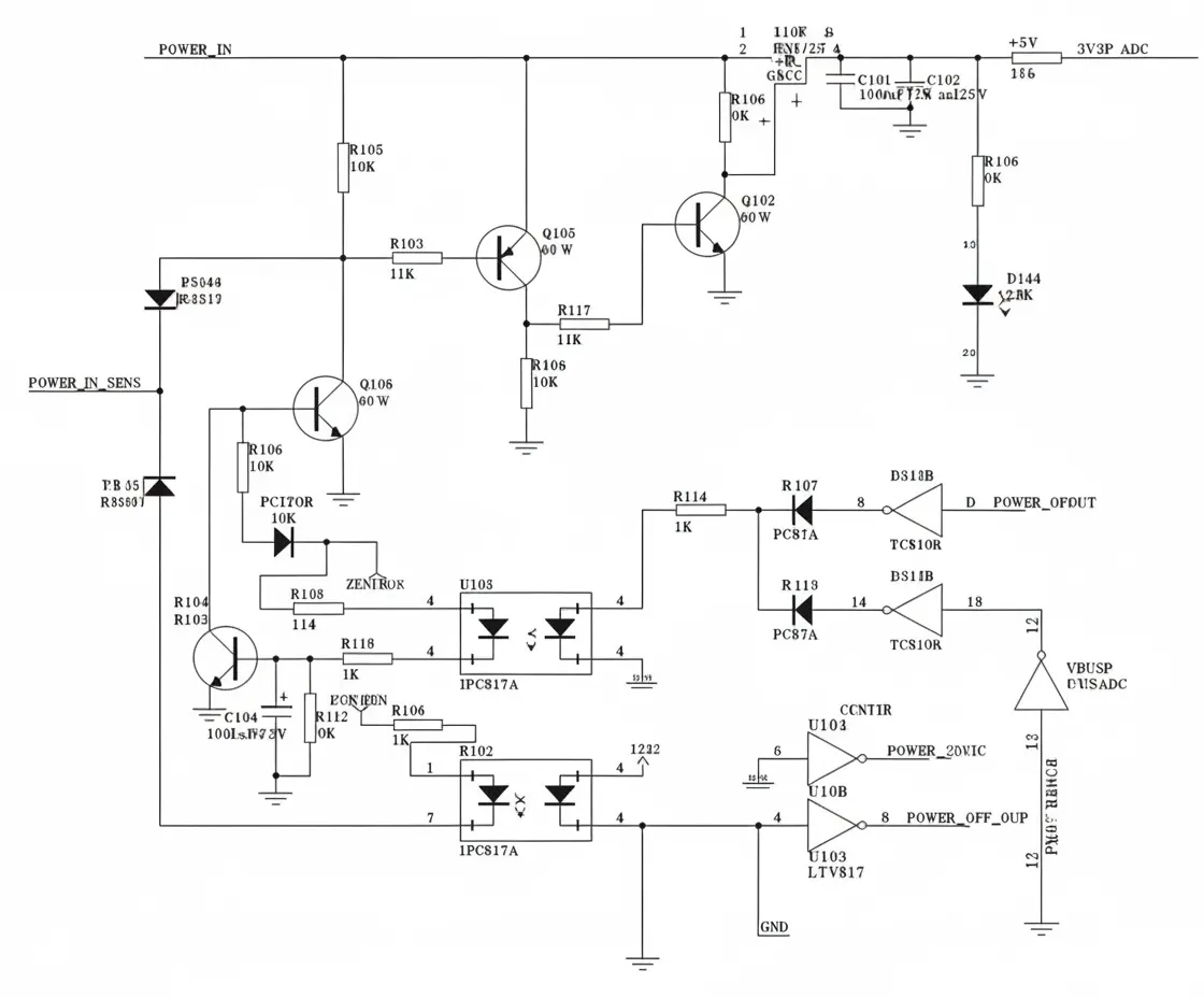
Figure 3 Single-key touch power on/off circuit
While the system is on, pressing POWER-KEY2 again causes optocoupler B101 to conduct. The optocoupler secondary conducts and the inverter D101 outputs a low level to the control panel. The control panel issues the POWER-OFF1 low-level shutdown command, which drives optocoupler B100, turning on transistor N103 and turning off N104. The resulting high level at N104 collector turns N106 off, which in turn turns Q100 off and powers the system down.
When the host PC issues a high-level POWER-OFF command, optocoupler B100 also conducts and the remaining shutdown sequence is the same as a control panel-initiated shutdown.
Low-voltage power circuits
The low-voltage power circuits are shown in Figure 4. The design uses six TI TPS5430 switching regulators and one National Semiconductor LM2576. The six TPS5430 devices produce two identical groups of +12 V, +5 V, and +3.3 V rails: one group supplies the ultrasound main control board and the other supplies the on-board computer. LM2576 is used to generate -12 V for the computer.
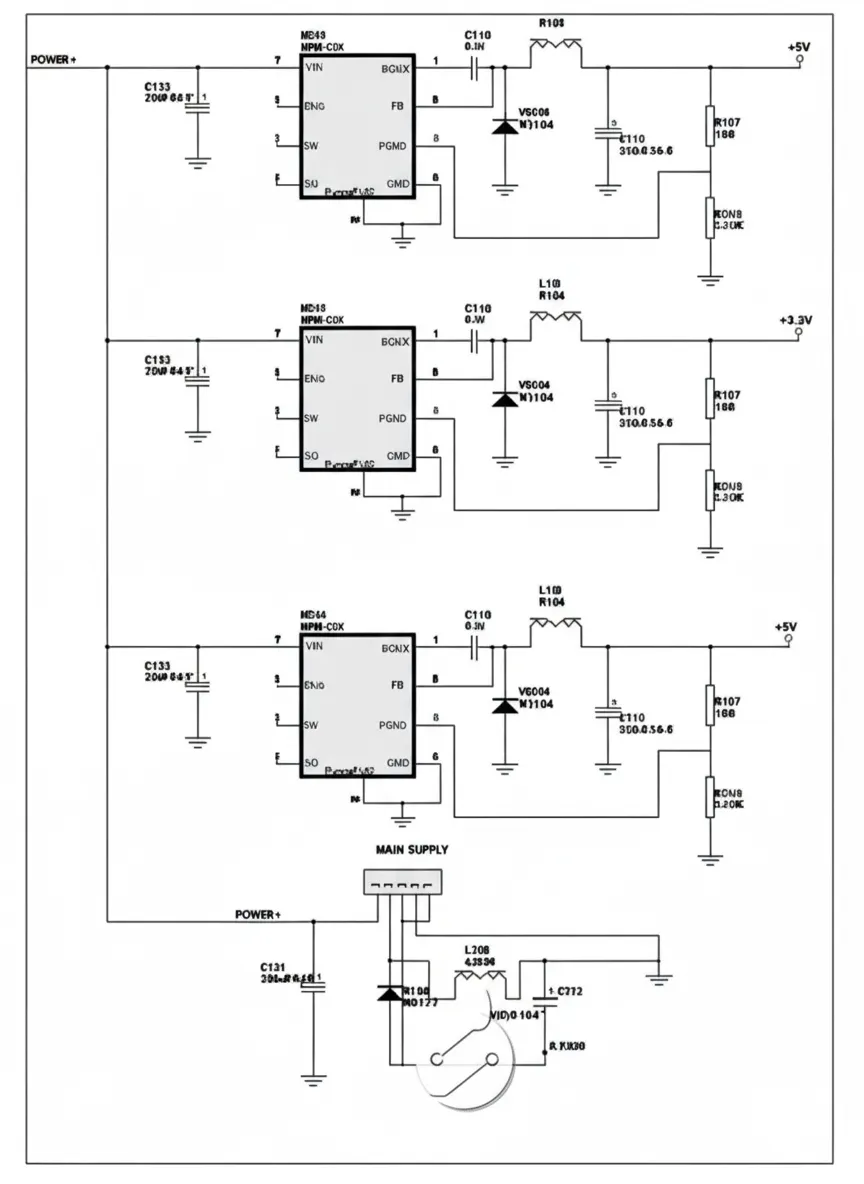
Figure 4 Low-voltage power circuit
TPS5430 accepts a 5.5 V to 36 V input range, provides continuous 3 A output current (4 A peak), and can reach up to 95% efficiency. It is available in an 8-pin small package with a PowerPad thermal pad on the back that must be soldered to ground on the PCB as the 9th pin for heat dissipation. No additional heatsink is required, making it suitable for portable designs. Pin 1 is BOOT and requires a 0.01 μF low-ESR capacitor between BOOT and pin 8 (PH). Pins 2 and 3 are no-connect. Pin 4 (VSENSE) is the feedback input and connects to the output divider. Pin 5 (ENA) is the enable input; driving it below 0.5 V shuts down the converter to 18 μA standby. The part is left floating to enable normal operation. Pin 6 is ground, and pin 7 (VIN) is the power input connected to POWER+. Place a high-quality low-ESR ceramic capacitor between VIN and ground. Pin 8 is PH, the switch node, which connects to the external catch diode and inductor. The PowerPad on the package must be tied to GND.
The TPS5430 output voltage is set by the divider on pin 4: Vout = (1.221 + (R1 * 1.221) / R2) V, where R1 is the upper divider resistor and R2 is the lower. For this design, R1 can be 10 kΩ and R2 is selected to obtain the desired output. Using R206 = 1.11 kΩ, R208 = 3.07 kΩ, and R210 = 5.36 kΩ yields output voltages of approximately 12.2 V, 5.2 V, and 3.5 V, about 0.2 V above nominal; under load, voltages settle to appropriate values.
Device N208 (LM2576-12) is from National Semiconductor. Pin 1 is VIN connected to POWER+; pin 2 is the output node that interfaces to the catch diode and inductor; pin 3 is ground; pin 5 is the ON/OFF control. Because a negative output is required, pins 3 and 5 are tied to the -12 V rail instead of ground. Pin 4 is the feedback pin. Using the fixed 12 V LM2576-12, pin 4 is grounded and no external feedback divider is required.
High-voltage power circuit
The ±48 V high-voltage supplies are implemented with a DC/DC converter controller. The UA3843 is a high-performance, fixed-frequency, current-mode controller optimized for DC/DC converter applications, providing PWM control, cycle-by-cycle current limiting, and voltage regulation with minimal external components.
Figure 5 ±48 V power circuit
1. PWM control
POWER+ supplies N1 (UA3843) pin 7 through resistor R34. Pin 4 with R36 and C33 forms the sawtooth oscillator. PWM pulses are output on pin 6 to control MOSFET V9 conduction time, which determines output voltage. Gate resistor R37 suppresses parasitic oscillation and should be placed close to the MOSFET gate. R37 must not be too large since it affects the MOSFET switching speed by altering the drive charge/discharge path for the gate capacitance.
The secondary windings 9 and 10 of the switching transformer feed rectifier VD14 and filter network C35, L7, C36 to form the +48 V rail for the probe. Secondaries 7 and 6 feed VD13 and C39, L8, C37 to form the -48 V rail. VD12, C34, and R38 form a snubber to absorb voltage spikes generated at V9 drain during switching transitions. When V9 turns off, the drain spike charges C34 through VD12, limiting the spike amplitude. C34 then discharges through R38 to prepare for the next cycle.
2. Cycle-by-cycle current limit
Pin 2 (FEEDBACK) of the UA3843 is the feedback voltage input and is compared to the internal reference (typically +2.5 V) by the error amplifier. In this design pin 2 is grounded and control is provided via the error amplifier output on pin 1. Pin 3 provides cycle-by-cycle current limit and controls PWM width. R47, R48, R14, and C32 on pin 3 form the current-limit network: during each oscillator cycle, when the primary current in transformer L6 peaks at the set threshold, the PWM pulse is terminated. The threshold is determined by the voltage at pin 1 (COMP), which is the error amplifier output. R14 and C32 filter high-frequency sampling spikes to ensure reliable cycle-by-cycle limiting. R47 and R48 are current-sense resistors that set the maximum output current; changing them adjusts the converter's current limit.
3. Voltage regulation
The UA3843 implements both current-mode control and voltage-loop regulation. The current sense signal is presented to pin 3 for current-loop control, while the error amplifier output on pin 1 is used as the reference for the current comparator, forming the voltage loop. Voltage regulation uses a TL431A reference (N2), an optocoupler B4 (TLP521), and resistors R31, VR7, R12, R32, etc. The optocoupler output current is converted into a voltage and applied to pin 1 of the UA3843. TL431A has a 2.5 V internal reference. As output voltage rises, TL431 conduction increases, the optocoupler conducts more, pin 1 voltage falls, the internal current comparator trips sooner, PWM pulses narrow, and the output voltage is reduced, stabilizing the output.
The high-voltage output is given by VOUT = (1 + R31 / (R12 + VR7)) * Vref. Adjusting potentiometer VR7 allows the ±48 V outputs to be set; the adjustment range in this design is approximately 77.5 V down to 32 V.
Conclusion
This article described the design of a portable ultrasound power supply, including the power source switching circuit, single-key touch power on/off circuit, low-voltage regulator designs, and high-voltage converter design. The implementation met the design requirements and can be applied to other portable devices.