ALLPCB


Why Pad-to-Pad Spacing Matters in SMT Assembly
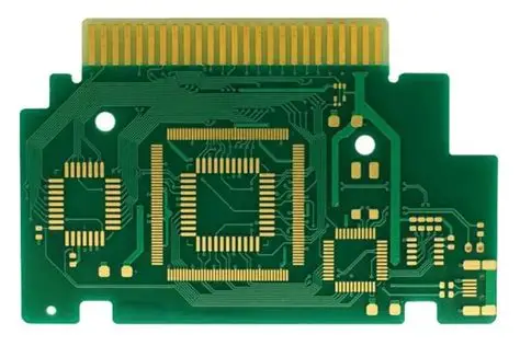
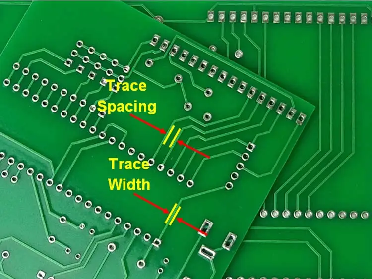
Pad-to-pad spacing refers to the distance between adjacent copper pads on a PCB intended for surface mount components. This dimension directly influences solder paste deposition, molten solder flow, and final joint formation. In reflow soldering, inadequate spacing often results in solder bridging between pads, creating electrical shorts. Conversely, excessive spacing may limit the formation of proper solder fillets, reducing mechanical strength and thermal conductivity of the joint. Following established smt assembly guidelines helps balance these factors for reliable outcomes. Industry standards emphasize that spacing decisions should account for component pitch, pad geometry, and the specific reflow profile used.
Technical Principles of Reflow Soldering Pad Spacing
During reflow, solder paste melts and flows under surface tension and gravity. The gap between pads determines how much solder can bridge or spread without creating defects. Narrow spacing increases the risk of bridging because molten solder can easily connect adjacent pads before cooling. Component floating, also known as tombstoning, becomes more likely when uneven heating or paste volume differences occur across closely spaced pads. Solder fillet formation depends on sufficient pad area and appropriate spacing to allow solder to climb the component termination properly. Stencil design for smt directly affects the volume of paste applied, making pad spacing and aperture alignment interdependent factors in achieving consistent joints.
Thermal expansion differences between the PCB and components during heating can further stress joints if spacing is not optimized. Standards such as those from IPC provide land pattern recommendations that incorporate tolerances for manufacturing variations. These guidelines help designers calculate minimum spacing values based on component dimensions and process capabilities. Proper spacing also supports better inspection access for automated optical inspection systems after reflow.
Common Pitfalls in Pad Spacing and Component Floating Prevention
One frequent issue arises when designers copy footprints without verifying spacing against the actual assembly process. This often leads to bridging on fine-pitch components where the gap falls below the minimum recommended by process capability studies. Component floating prevention requires balanced paste volumes on all terminations, which becomes harder to achieve with inconsistent pad spacing. Another pitfall involves ignoring the effects of PCB warpage during reflow, which can alter effective spacing and cause uneven solder flow.

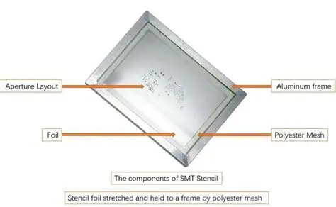
Stencil design for smt must align apertures precisely with pad edges to avoid paste smearing into the gap. Overly aggressive reduction of spacing to save board space frequently compromises yield. Engineers should evaluate spacing not only at the design stage but also through prototype builds that simulate production reflow conditions.
Best Practices and Stencil Design for SMT
Start by consulting land pattern standards that define minimum and nominal spacing values for various component families. Adjust these base values upward when using thicker stencils or higher-viscosity pastes to maintain adequate separation. For component floating prevention, ensure symmetric pad layouts and consistent thermal relief connections where needed. Stencil thickness and aperture shape should be selected to deliver paste volumes that fill the joint without excess that could bridge narrow gaps.
Review the full reflow profile, including ramp rates and peak temperatures, because these influence how far solder can flow. Collaborate with assembly partners early to incorporate their specific equipment tolerances into spacing decisions. Document all spacing choices and rationale in design files to support future revisions or troubleshooting.
Troubleshooting Insights for SMT Assembly
When bridging occurs, measure actual pad spacing on production boards and compare against design intent. Insufficient spacing combined with excess paste volume is a common root cause. For weak or incomplete fillets, check whether spacing allows adequate solder wicking up the component leads. Process adjustments such as slight reductions in paste volume or modifications to the reflow peak can sometimes compensate for marginal spacing, but redesign remains the most reliable long-term solution.
Regular audits of stencil condition and alignment help maintain consistent results over high-volume runs. Tracking defect rates by component type often reveals spacing-related patterns that guide targeted improvements.
Conclusion
Careful management of pad-to-pad spacing forms a foundational element of successful SMT assembly. By understanding the mechanisms of solder flow, fillet formation, and defect generation, engineers can make informed layout decisions that improve yield and reliability. Integrating these considerations with appropriate stencil design for smt and adherence to recognized assembly guidelines reduces the likelihood of costly rework or field failures. Consistent application of these principles supports high-quality outcomes across diverse product portfolios.
FAQs
Q1: What minimum pad-to-pad spacing should be used in smt assembly guidelines?
A1: Recommended spacing depends on component pitch and land pattern standards, with typical values starting from 0.2 mm or more for fine-pitch parts. Designers should verify against specific component datasheets and process capabilities to prevent bridging while allowing proper solder fillet formation.
Q2: How does reflow soldering pad spacing affect component floating prevention?
A2: Adequate and balanced spacing helps maintain even heating and paste volume across terminations, reducing the torque that causes components to stand on end. Uneven spacing can exacerbate floating by creating differential surface tension during reflow.
Q3: Why is stencil design for smt critical when pad spacing is tight?
A3: Stencil apertures must precisely control paste volume to avoid excess material flowing into narrow gaps. Poor stencil design can lead to bridging or insufficient solder even when pad spacing meets nominal guidelines.
Q4: What role does solder fillet formation play in overall joint reliability?
A4: Proper fillet formation requires sufficient pad spacing to allow solder to wet and climb the component termination fully. Inadequate spacing restricts fillet development and can compromise both mechanical strength and electrical performance of the joint.