ALLPCB


If you're designing a high-frequency PCB for ultrasound transducers, you're likely wondering how to ensure signal integrity, minimize loss, and achieve precise impedance matching. The answer lies in careful layout planning, material selection, and adherence to specific design rules tailored for high-frequency signals. In this guide, we'll dive deep into the essentials of high-frequency PCB design rules for ultrasound applications, covering impedance matching, signal integrity, and strategies for minimizing signal loss. Whether you're a seasoned engineer or new to ultrasound PCB design, this comprehensive resource will help you optimize your layout for peak performance.
Introduction to High-Frequency PCB Design for Ultrasound Transducers
Ultrasound transducers operate at high frequencies, often in the range of 1 MHz to 20 MHz or higher, depending on the application. These frequencies are used in medical imaging, industrial testing, and other precision systems. Designing a PCB for such devices requires special attention to signal integrity and minimizing interference, as even small errors can degrade performance or distort the ultrasound signal.
High-frequency PCB design for ultrasound isn't just about connecting components—it's about managing electromagnetic behavior, controlling impedance, and ensuring that signals travel without significant loss or distortion. In this guide, we'll break down the critical aspects of optimizing your PCB layout for ultrasound transducers, focusing on practical tips and proven strategies.
Why High-Frequency PCB Design Rules Matter for Ultrasound
Ultrasound transducers rely on high-frequency signals to generate and detect sound waves. At these frequencies, signal behavior changes dramatically compared to low-frequency circuits. Issues like crosstalk, reflections, and signal loss become more pronounced, making strict design rules essential.
For instance, a mismatch in impedance can cause signal reflections, reducing the clarity of the ultrasound image. Similarly, poor grounding can introduce noise, interfering with the transducer's ability to detect faint echoes. By following high-frequency PCB design rules for ultrasound, you can avoid these pitfalls and ensure reliable performance. Let's explore the key areas to focus on.
Key High-Frequency PCB Design Rules for Ultrasound Transducers
1. Material Selection for High-Frequency Performance
The choice of PCB material directly impacts signal integrity in ultrasound designs. Standard FR-4 materials may not suffice for high-frequency applications due to their higher dielectric loss and inconsistent dielectric constant at frequencies above a few MHz.
Instead, consider using low-loss materials like Rogers RO4350B or Isola IS680, which offer stable dielectric properties and lower signal attenuation at frequencies up to 20 MHz or higher. These materials help maintain signal strength and reduce distortion, critical for ultrasound imaging accuracy. While they are more expensive, the performance benefits often justify the cost in precision applications.
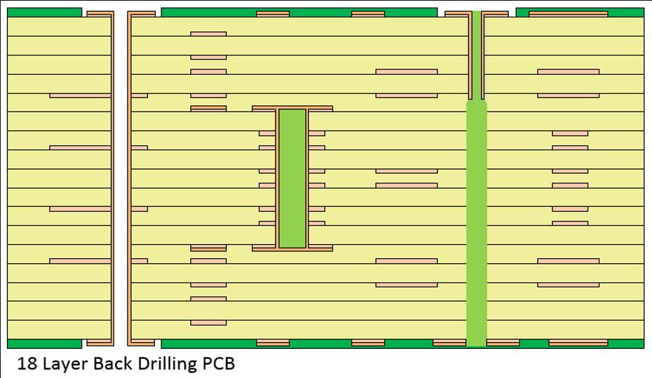
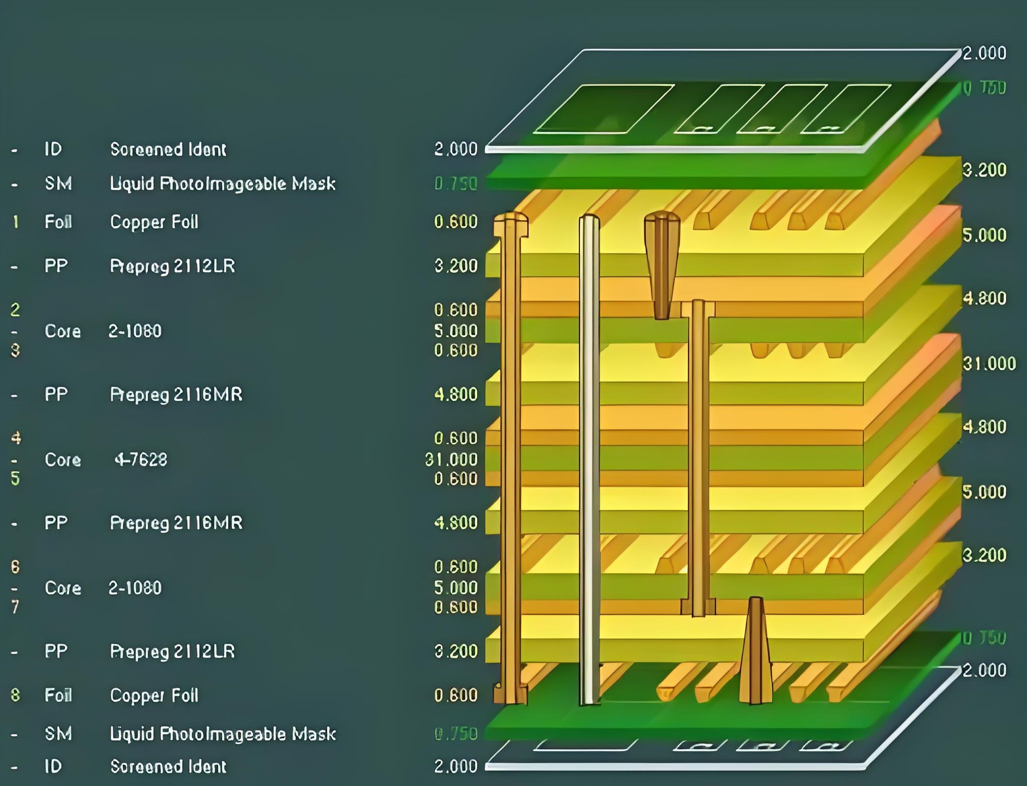
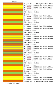
2. Layer Stack-Up for Signal Isolation
A well-planned layer stack-up is vital for managing high-frequency signals. For ultrasound PCBs, a multilayer design (4 or more layers) is often necessary to separate signal, power, and ground planes effectively. A common stack-up might include:
- Top Layer: Signal traces for transducer connections
- Layer 2: Ground plane for shielding
- Layer 3: Power distribution
- Bottom Layer: Additional signal traces or ground
This configuration minimizes crosstalk between signal lines and provides a low-impedance return path for high-frequency currents. Ensure that ground planes are continuous under signal traces to avoid interruptions that could cause signal reflections.
3. Trace Width and Spacing for High-Frequency Signals
Trace design is critical in high-frequency PCB layouts. At ultrasound frequencies, traces act more like transmission lines than simple conductors. Use a trace width calculator to determine the appropriate dimensions based on your PCB material's dielectric constant and the desired characteristic impedance, typically 50 ohms for many ultrasound systems.
For example, on a material with a dielectric constant of 3.5, a 50-ohm trace might be around 0.3 mm wide for a 1.6 mm thick substrate. Keep spacing between adjacent traces at least 3 times the trace width to reduce crosstalk. Avoid sharp corners in traces—use 45-degree angles or curves to prevent signal reflections.
Impedance Matching for Ultrasound PCB Design
Impedance matching is a cornerstone of high-frequency design, especially for ultrasound transducers. A mismatch between the transducer, traces, and connected components can lead to signal reflections, reducing the efficiency of energy transfer and degrading image quality.
Understanding Impedance in Ultrasound Systems
Ultrasound transducers often have specific impedance values, typically ranging from 50 to 100 ohms, depending on the design. The PCB traces and connectors must match this impedance to ensure maximum power transfer. Mismatches as small as 10% can cause noticeable signal loss.
Techniques for Impedance Matching
To achieve proper impedance matching for ultrasound PCB designs:
- Use Controlled Impedance Traces: Design traces with a consistent width and spacing to maintain the target impedance (e.g., 50 ohms). Use PCB design software with built-in impedance calculators for accuracy.
- Add Matching Networks: If direct matching isn't possible, incorporate passive components like capacitors and inductors near the transducer to form a matching network. For instance, a series inductor and shunt capacitor can adjust impedance at specific frequencies like 5 MHz.
- Minimize Via Usage: Vias introduce inductance and can disrupt impedance. If unavoidable, use multiple vias in parallel to reduce their impact.
Signal Integrity in Ultrasound PCB Design
Signal integrity ensures that the high-frequency pulses sent to and received from the transducer remain clear and undistorted. Poor signal integrity can result in noise, jitter, or loss of critical data, directly affecting ultrasound performance.
Grounding for Noise Reduction
A solid grounding strategy is essential for maintaining signal integrity in ultrasound PCB design. Use a dedicated ground plane beneath signal traces to provide a low-impedance return path. Avoid splitting the ground plane under high-frequency traces, as this can create loops that pick up electromagnetic interference (EMI).
Place decoupling capacitors (e.g., 0.1 μF ceramic capacitors) close to power pins of active components to filter out high-frequency noise. Keep the loop area between the capacitor and the IC as small as possible by placing vias directly next to the pads.
Shielding and Isolation
Ultrasound signals are sensitive to external interference. Use shielding techniques such as guard traces or copper pours around critical signal lines to isolate them from noise sources. If your design includes digital and analog sections, keep them on separate layers or zones to prevent digital switching noise from affecting analog ultrasound signals.
Minimizing Signal Loss in Ultrasound PCB Layouts
Signal loss is a major concern in high-frequency designs, as it reduces the strength of the ultrasound signal and impacts system sensitivity. Here are actionable strategies for minimizing signal loss in ultrasound PCB designs.
Shorten Trace Lengths
Long traces increase resistance and capacitance, leading to signal attenuation. Keep traces between the transducer and driving circuitry as short as possible. For example, aim for trace lengths under 10 mm for signals at 10 MHz to limit loss to less than 0.5 dB.
Use Low-Loss Materials
As mentioned earlier, high-frequency materials with low dielectric loss tangents (e.g., below 0.003) help minimize signal attenuation. Compare this to standard FR-4, which can have a loss tangent of 0.02, causing significant signal degradation above 5 MHz.
Avoid Unnecessary Connectors
Connectors introduce insertion loss and impedance discontinuities. If possible, solder the transducer directly to the PCB. If connectors are required, choose high-frequency rated ones with minimal loss specifications (e.g., less than 0.2 dB at 10 MHz).
Thermal Management in High-Frequency Ultrasound PCBs
Ultrasound transducers and their driving circuits can generate significant heat, especially in continuous-wave applications. Poor thermal management can alter component performance and degrade signal integrity.
Incorporate thermal vias under high-power components to transfer heat to inner or bottom layers. Use copper pours as heat sinks where space allows, and ensure adequate airflow in the final enclosure. For example, a driver IC dissipating 2 watts might require a 10 mm x 10 mm copper area with 4-6 thermal vias for effective cooling.
Testing and Validation of Ultrasound PCB Designs
After completing your PCB layout, thorough testing is crucial to verify performance. Use a network analyzer to measure impedance at key points, ensuring it matches the transducer's specifications (e.g., within ±5% of 50 ohms). Perform signal integrity tests with an oscilloscope to check for reflections or noise in the ultrasound pulses.
Additionally, simulate real-world conditions by testing the PCB with the actual transducer under load. Measure parameters like signal-to-noise ratio (SNR) and ensure it meets or exceeds the required threshold for your application, such as 40 dB for medical imaging.
Common Mistakes to Avoid in Ultrasound PCB Design
Even experienced designers can make errors in high-frequency layouts. Here are some pitfalls to watch out for:
- Ignoring Impedance Control: Failing to design for controlled impedance can cause significant signal reflections.
- Poor Component Placement: Placing sensitive components near noisy power supplies can introduce interference.
- Inadequate Grounding: A broken or poorly designed ground plane can lead to EMI and signal degradation.
Conclusion: Building Better Ultrasound PCBs with High-Frequency Design
Optimizing a high-frequency PCB layout for ultrasound transducers requires a blend of technical precision and strategic planning. By adhering to high-frequency PCB design rules for ultrasound, focusing on impedance matching, ensuring signal integrity, and minimizing signal loss, you can create a reliable and efficient design that meets the demanding needs of ultrasound applications.
Start with the right materials and stack-up, design traces for controlled impedance, and prioritize short, direct connections to reduce loss. Test thoroughly to validate your design, and avoid common mistakes that could compromise performance. With these strategies, you'll be well-equipped to build high-performing PCBs for ultrasound systems.
At ALLPCB, we're committed to supporting engineers with the tools and resources needed for cutting-edge designs. Whether you're prototyping or scaling to production, our expertise in high-frequency PCB manufacturing can help bring your ultrasound projects to life.