In the world of electronics, high-frequency printed circuit boards (PCBs) are at the heart of many cutting-edge devices, from wireless communication systems to high-speed digital circuits. However, as frequencies increase, so does the risk of electromagnetic interference (EMI), which can disrupt performance and cause signal integrity issues. So, how can you minimize EMI in high-frequency PCBs? The key lies in smart layout techniques, effective shielding, and strategic component placement.
In this comprehensive guide, we’ll explore practical methods to reduce EMI in high-frequency PCB designs. From grounding strategies to the use of decoupling capacitors and Faraday cages, we’ll dive into actionable tips that engineers can apply to ensure optimal performance and compliance with EMI regulations. Whether you’re designing for 5G, IoT, or other high-speed applications, these techniques will help you tackle EMI challenges head-on.
Understanding EMI in High-Frequency PCBs
Electromagnetic interference occurs when unwanted electromagnetic fields disrupt the operation of electronic devices. In high-frequency PCBs, where signals switch at rates often exceeding 1 GHz, EMI becomes a significant concern. These fast-switching signals can generate noise that radiates or conducts through traces, power planes, or even nearby components, leading to crosstalk, signal degradation, or failure to meet regulatory standards.
The sources of EMI in high-frequency designs include:
- Rapid signal transitions creating harmonic noise.
- Improper grounding leading to ground loops or noise coupling.
- Poor trace routing causing crosstalk between adjacent lines.
- Inadequate shielding allowing external or internal interference.
To combat these issues, a combination of layout design techniques and shielding methods is essential. Let’s break down the most effective strategies for high-frequency PCB EMI shielding and interference reduction.
Key Layout Techniques for EMI Reduction
A well-thought-out PCB layout is the first line of defense against EMI. Below are proven techniques to minimize interference in high-frequency designs.
1. Optimize PCB Grounding Techniques
Grounding is critical in high-frequency PCB designs as it provides a low-impedance path for return currents, reducing noise and preventing ground loops. Poor grounding can amplify EMI by allowing noise to couple into sensitive circuits. Here are some essential PCB grounding techniques to follow:
- Use a Solid Ground Plane: A continuous ground plane on one layer of the PCB helps minimize impedance and provides a stable reference for signals. For multilayer boards, dedicate an entire layer to ground to reduce noise coupling.
- Avoid Ground Splits: Splitting ground planes under high-frequency traces can create discontinuities in return paths, increasing EMI. If splits are unavoidable, use stitching capacitors (e.g., 0.1 μF) to bridge the gap at high frequencies.
- Star Grounding for Analog and Digital Sections: Separate analog and digital ground planes and connect them at a single point (star grounding) to prevent digital noise from interfering with sensitive analog signals.
By ensuring low-impedance grounding, you can significantly reduce conducted EMI. For example, a ground plane with a thickness of 1 oz copper can handle return currents for signals up to 2 GHz without significant voltage drops.
2. Implement Guard Traces for EMI Reduction
Guard traces are an effective way to isolate high-frequency signals and prevent crosstalk, a common source of EMI. These are grounded traces placed parallel to sensitive signal lines to act as a barrier against electromagnetic coupling.
- Placement: Position guard traces on both sides of critical high-speed traces, especially for clock signals or data lines operating above 500 MHz.
- Grounding: Connect guard traces to the ground plane at multiple points using vias spaced at intervals of λ/20 (where λ is the wavelength of the highest frequency signal) to ensure effective shielding.
- Width and Spacing: Make guard traces at least as wide as the signal trace, and maintain a spacing of 3 times the trace width between the signal and guard trace to minimize coupling.
Using guard traces for EMI reduction can lower crosstalk by up to 20 dB in high-density layouts, ensuring cleaner signal transmission in high-frequency applications.
3. Strategic Use of Decoupling Capacitors in High-Frequency Designs
Decoupling capacitors are vital for stabilizing power supply lines and reducing noise in high-frequency circuits. They act as local energy storage, providing instantaneous current to components during fast switching, thus preventing voltage fluctuations that contribute to EMI.
- Capacitor Selection: For decoupling capacitors in high-frequency designs, choose ceramic capacitors with low equivalent series inductance (ESL) and values ranging from 0.01 μF to 0.1 μF for frequencies above 100 MHz.
- Placement: Place decoupling capacitors as close as possible to the power pins of ICs, ideally within 1-2 mm, to minimize loop inductance. Use multiple capacitors in parallel for different frequency ranges if needed.
- Via Design: Connect capacitors to power and ground planes with short, wide vias to reduce parasitic inductance, which can degrade performance at frequencies above 1 GHz.
For instance, in a 2.4 GHz Wi-Fi module design, placing a 0.1 μF capacitor near each power pin of the RF IC can suppress noise by up to 30 dB, ensuring stable operation.
4. Proper Trace Routing and Impedance Control
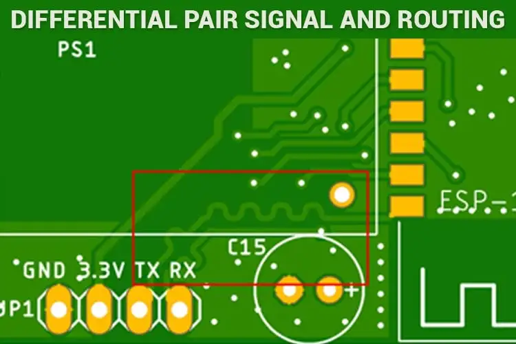
High-frequency signals are highly sensitive to trace length, width, and routing paths. Improper routing can lead to signal reflections, crosstalk, and radiated EMI. Follow these guidelines for optimal trace design:
- Controlled Impedance: Design traces to match the characteristic impedance of the system (e.g., 50 ohms for RF signals) to prevent reflections. Use trace width calculators to achieve the desired impedance based on dielectric thickness and material (e.g., FR-4 with εr = 4.2).
- Minimize Trace Length: Keep high-frequency signal traces as short as possible to reduce parasitic capacitance and inductance. For a 1 GHz signal, a trace longer than 1 inch can introduce significant delay and noise.
- Avoid 90-Degree Bends: Use 45-degree angles or curved traces to prevent impedance discontinuities and reduce radiated EMI at sharp corners.
By maintaining controlled impedance and minimizing trace length, you can ensure signal integrity and reduce EMI in high-speed designs.
Advanced EMI Shielding Techniques
Beyond layout optimization, physical shielding methods play a crucial role in protecting high-frequency PCBs from external and internal interference. Let’s explore two powerful approaches.
1. Faraday Cage in PCB Design
A Faraday cage is a conductive enclosure that blocks external electromagnetic fields, making it an excellent solution for Faraday cage PCB design in high-frequency applications. This technique is particularly useful for RF circuits or sensitive analog sections.
- Implementation: Create a Faraday cage by surrounding the sensitive area with a grounded copper shield, either as a metal can soldered to the PCB or as a series of closely spaced vias (via fence) connected to ground planes on multiple layers.
- Via Spacing: Space vias at intervals of λ/20 or less (e.g., 1.5 mm for a 10 GHz signal) to prevent electromagnetic waves from passing through gaps.
- Applications: Use Faraday cages around RF transceivers or high-speed ADCs to shield them from external EMI sources like nearby cellular signals or power line noise.
A properly implemented Faraday cage can attenuate external EMI by 40-60 dB, ensuring reliable operation in noisy environments.
2. EMI Shielding Materials and Layers
In addition to layout and Faraday cages, using specialized materials can enhance high-frequency PCB EMI shielding. These include:
- Shielding Films: Apply conductive films or coatings over sensitive areas to block radiated EMI. These are often used in flexible PCBs or compact designs.
- Copper Layers: Incorporate additional copper layers in multilayer boards to act as shields between high-frequency signal layers.
- Metal Enclosures: Enclose the entire PCB or critical sections in a grounded metal housing to provide robust protection against external interference.
Selecting the right shielding material depends on the frequency range and design constraints. For example, a thin conductive film can provide 20-30 dB of shielding for frequencies up to 5 GHz without adding significant weight to the design.
Additional Tips for EMI Compliance
Beyond layout and shielding, consider these practices to ensure your high-frequency PCB meets EMI standards:
- Component Placement: Group high-frequency components together and away from sensitive analog circuits to minimize interference. Place noisy components like switching regulators far from RF sections.
- Filtering: Use low-pass filters or ferrite beads on power lines to suppress high-frequency noise before it reaches sensitive ICs.
- Simulation Tools: Leverage PCB design software with EMI simulation capabilities to predict and mitigate interference during the design phase.
- Testing: Perform pre-compliance EMI testing using a spectrum analyzer to identify and address radiated or conducted noise early in the development cycle.
Conclusion: Building EMI-Resistant High-Frequency PCBs
Designing high-frequency PCBs that minimize EMI requires a combination of careful layout planning, strategic component placement, and effective shielding. By implementing PCB grounding techniques, using guard traces for EMI reduction, placing decoupling capacitors for high-frequency noise suppression, and incorporating Faraday cage PCB design, you can significantly improve signal integrity and ensure compliance with regulatory standards.
Start with a solid ground plane, optimize trace routing, and shield sensitive areas to protect your design from both internal and external interference. With these practical techniques for high-frequency PCB EMI shielding, you’ll be well-equipped to tackle the challenges of modern high-speed electronics and deliver reliable, high-performance products.
Apply these strategies in your next project to see the difference in performance and reliability. With the right approach, EMI doesn’t have to be a roadblock in your high-frequency PCB designs.
 ALLPCB


