If you're designing a printed circuit board (PCB) and wondering which stackup configuration—such as a 4-layer stackup, 6-layer stackup, or 8-layer stackup—is best for your project, you're in the right place. Each PCB stackup has unique advantages and challenges, especially when it comes to high-speed design. In this blog, we'll break down the pros and cons of these configurations to help you choose the right one for your needs. We'll dive deep into each type, providing practical insights for engineers and designers looking to optimize performance, cost, and manufacturability.
What Is a PCB Stackup and Why Does It Matter?
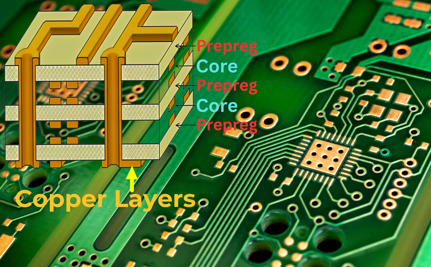
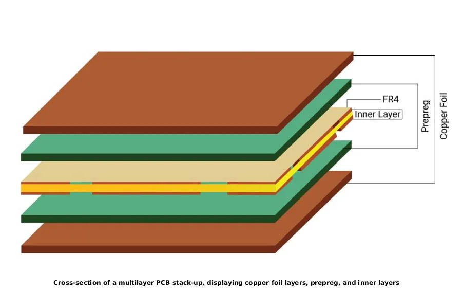
A PCB stackup refers to the arrangement of conductive copper layers and insulating materials (like prepreg and core) in a multilayer PCB. These layers are carefully organized to handle signals, power distribution, and grounding. The stackup design directly impacts signal integrity, electromagnetic interference (EMI), thermal management, and manufacturing costs. For applications like high-speed design, where signals travel at rapid rates, the stackup can make or break your board's performance.
Choosing the right stackup—whether it's a 4-layer stackup for simpler designs or an 8-layer stackup for complex, high-speed systems—depends on your project's requirements. Let's explore the specifics of each configuration to understand their strengths and limitations.
4-Layer Stackup: A Cost-Effective Choice for Simpler Designs
A 4-layer stackup is one of the most common configurations for PCB designs that need more complexity than a 2-layer board but don't require the advanced features of higher-layer counts. It typically consists of two signal layers on the outer sides and two inner layers dedicated to power and ground planes.
Pros of a 4-Layer Stackup
- Cost-Effective: A 4-layer stackup is relatively inexpensive compared to higher-layer configurations. It offers a good balance between functionality and manufacturing cost, making it ideal for small to medium-scale projects.
- Improved Signal Integrity: With dedicated ground and power planes, a 4-layer stackup reduces noise and crosstalk compared to 2-layer boards. This is especially useful for designs with moderate signal speeds, typically up to 100 MHz.
- Compact Design: The additional layers allow for denser routing in a smaller footprint, which is great for compact devices like consumer electronics.
- EMI Control: The ground plane helps shield signals from external interference and reduces EMI, a critical factor even in simpler designs.
Cons of a 4-Layer Stackup
- Limited Routing Space: With only two signal layers, complex designs with many components can quickly run out of routing space, leading to potential design compromises.
- Not Ideal for High-Speed Design: For applications exceeding 100-200 MHz, a 4-layer stackup may struggle with signal integrity issues due to longer trace lengths and limited layer options for controlled impedance.
- Thermal Limitations: With fewer layers to distribute heat, high-power applications may face thermal management challenges.
When to Use: A 4-layer stackup is best for simpler designs, such as basic microcontrollers, low-speed digital circuits, or compact IoT devices. If your project involves high-speed design, you might need to consider more layers for better performance.
6-Layer Stackup: Stepping Up for Moderate Complexity and High-Speed Design
A 6-layer stackup adds two more layers to the 4-layer design, typically providing additional signal layers or mixed configurations for power and ground. This setup is often used in designs that require better signal integrity and more routing options, especially for high-speed design applications.
Pros of a 6-Layer Stackup
- Better Routing Flexibility: With four signal layers (in a common configuration like Signal-Ground-Signal-Signal-Power-Signal), a 6-layer stackup offers more space for complex routing, accommodating densely packed components.
- Enhanced Signal Integrity for High-Speed Design: The additional layers allow for controlled impedance traces, which are critical for high-speed signals (e.g., above 200 MHz). For instance, differential pairs can be routed with precise impedance matching, often around 50 ohms for single-ended signals or 100 ohms for differential pairs.
- Improved EMI Shielding: Multiple ground planes can sandwich signal layers, reducing crosstalk and external interference—a must for sensitive high-speed circuits.
- Thermal Management: Additional layers provide more copper area for heat dissipation, which is beneficial for designs with moderate power requirements.
Cons of a 6-Layer Stackup
- Higher Cost: Manufacturing a 6-layer stackup is more expensive than a 4-layer due to increased material and processing complexity. This can impact budget-sensitive projects.
- Design Complexity: More layers mean more planning for via placement, layer transitions, and impedance control. Errors in stackup design can lead to signal degradation or manufacturing issues.
- Still Limited for Ultra-High-Speed: While suitable for many high-speed designs, extremely fast signals (e.g., above 1 GHz) or very complex systems may require even more layers for optimal performance.
When to Use: A 6-layer stackup shines in applications like telecommunications, moderate high-speed digital circuits, and advanced microcontrollers. If your project involves high-speed design with frequencies in the hundreds of megahertz, this configuration often provides the right balance of performance and cost.
8-Layer Stackup: Advanced Performance for Complex High-Speed Design
An 8-layer stackup is a go-to choice for complex designs that demand superior signal integrity, extensive routing, and robust power distribution. This configuration typically includes multiple signal layers, dedicated ground planes, and power planes, making it ideal for cutting-edge high-speed design.
Pros of an 8-Layer Stackup
- Maximum Routing Capacity: With up to six signal layers in some configurations (e.g., Signal-Ground-Signal-Power-Signal-Ground-Signal-Signal), an 8-layer stackup supports highly dense and intricate designs, perfect for multi-chip modules or advanced processors.
- Superior Signal Integrity for High-Speed Design: This stackup excels in managing ultra-high-speed signals, often exceeding 1 GHz. It allows for precise impedance control (e.g., maintaining 50-ohm traces with minimal deviation) and shorter signal paths through strategic via placement.
- Excellent EMI Control: Multiple ground planes can fully shield sensitive signal layers, minimizing crosstalk and external noise—a critical feature for RF and high-speed digital applications.
- Robust Power Distribution: Dedicated power planes ensure stable voltage delivery to components, even in power-hungry systems, reducing voltage drops and noise.
Cons of an 8-Layer Stackup
- High Cost: The manufacturing cost for an 8-layer stackup is significantly higher due to the increased number of layers, materials, and fabrication complexity. This can be a barrier for smaller projects or prototypes.
- Complex Design Process: Designing an 8-layer PCB requires advanced expertise in stackup planning, via optimization, and impedance matching. Mistakes can lead to costly redesigns or performance issues.
- Thicker Boards: More layers often result in a thicker PCB, which may not fit in space-constrained applications or may require specialized enclosures.
When to Use: An 8-layer stackup is ideal for advanced applications such as high-speed networking equipment, server boards, and RF systems where signal speeds exceed 1 GHz. If your project pushes the limits of high-speed design, this configuration offers the performance you need.
Comparing 4-Layer, 6-Layer, and 8-Layer Stackups for High-Speed Design
High-speed design is a critical factor in modern electronics, where signal integrity and minimal latency are paramount. Here's how the three stackup configurations compare in this context:
- 4-Layer Stackup: Suitable for low to moderate speeds (up to 100-200 MHz). It struggles with controlled impedance and EMI shielding for faster signals due to limited layers.
- 6-Layer Stackup: A strong choice for moderate high-speed design (200 MHz to 1 GHz). It supports controlled impedance and better shielding with additional signal and ground layers.
- 8-Layer Stackup: The best option for ultra-high-speed design (above 1 GHz). It provides maximum flexibility for impedance matching, signal isolation, and power stability.
For high-speed design, the choice often comes down to balancing performance with cost. A 6-layer stackup is frequently a sweet spot for many engineers, offering significant improvements over a 4-layer design without the hefty price tag of an 8-layer board. However, for cutting-edge applications like 5G or advanced computing, an 8-layer stackup is often non-negotiable.
Factors to Consider When Choosing a PCB Stackup Configuration
Selecting the right stackup for your project involves evaluating several key factors. Here's what to keep in mind:
- Signal Speed: Determine the frequency of your signals. For low-speed designs, a 4-layer stackup may suffice, while high-speed design often requires 6 or 8 layers.
- Component Density: High-density designs with many components need more routing space, pushing you toward a 6-layer or 8-layer stackup.
- Budget: Higher layer counts increase costs. Weigh the performance benefits against your budget constraints.
- EMI Requirements: If your design is sensitive to interference, prioritize stackups with multiple ground planes for shielding.
- Thermal Needs: Power-intensive designs benefit from additional layers to spread heat, favoring 6-layer or 8-layer configurations.
By carefully assessing these factors, you can choose a stackup that aligns with your technical and financial goals.
Practical Tips for Designing Your PCB Stackup
Designing a PCB stackup requires attention to detail to ensure optimal performance. Here are some actionable tips:
- Plan Layer Arrangement: Place ground planes adjacent to signal layers to minimize noise. For high-speed design, keep critical traces close to a reference plane for consistent impedance.
- Control Impedance: Use design tools to calculate trace widths and spacing for target impedance values (e.g., 50 ohms for single-ended signals). This is especially important for 6-layer and 8-layer stackups in high-speed applications.
- Minimize Via Transitions: Excessive via transitions can degrade signal quality in high-speed design. Route signals on the same layer when possible, especially in 4-layer designs with limited options.
- Work with Your Manufacturer: Collaborate early with your PCB fabricator to confirm stackup feasibility, material choices, and layer thicknesses. Standard thicknesses for a 4-layer board might be 1.6mm, while 8-layer boards could reach 2.0mm or more.
Conclusion: Finding the Right PCB Stackup for Your Project
Choosing between a 4-layer stackup, 6-layer stackup, or 8-layer stackup depends on the specific needs of your project. A 4-layer stackup offers affordability and simplicity for basic designs, while a 6-layer stackup steps up performance for moderate high-speed design. For the most demanding applications, an 8-layer stackup provides unmatched signal integrity and routing capacity, making it the top choice for ultra-high-speed systems.
Understanding the pros and cons of each configuration empowers you to make informed decisions that balance performance, cost, and manufacturability. Whether you're working on a compact IoT device or a cutting-edge networking system, the right PCB stackup is key to success. Take the time to evaluate your requirements, and don't hesitate to consult with experts or your manufacturing partner to finalize your design.
By leveraging the insights in this guide, you're well-equipped to navigate the complexities of PCB stackup configurations and achieve optimal results for your next project.
 ALLPCB


