ALLPCB


In the fast-evolving world of IoT (Internet of Things), designing compact, efficient, and cost-effective devices is a top priority. One powerful solution to achieve a small PCB footprint while maintaining performance is the use of Via-in-Pad (VIP) technology. This blog explores how VIP can reduce PCB size in IoT devices, focusing on strategies for IoT PCB design, wireless connectivity, low power consumption, and cost-effective solutions. Whether you're an engineer or a product developer, you'll find practical insights to optimize your next IoT project.
At ALLPCB, we understand the challenges of fitting advanced functionality into tiny spaces. Let’s dive into the details of VIP technology and how it can transform your IoT PCB designs.
Why Small PCB Footprint Matters in IoT Devices
IoT devices, such as smart sensors, wearables, and home automation gadgets, are often constrained by size. A smaller PCB footprint means more room for other components, sleeker product designs, and even lower manufacturing costs. However, shrinking a PCB without sacrificing performance is a complex task. Challenges include maintaining signal integrity, managing power consumption, and ensuring reliable wireless communication.
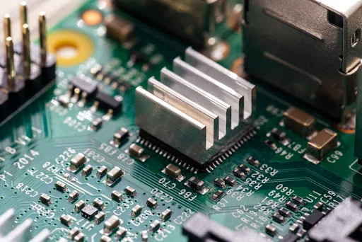
Traditional PCB layouts often waste space due to the placement of vias (vertical interconnect access) outside the component pads. This leads to larger boards and longer signal paths, which can degrade performance in high-speed IoT applications. This is where Via-in-Pad technology comes in as a game-changer, allowing designers to place vias directly under component pads, significantly reducing the board size.
What Is Via-in-Pad (VIP) Technology?
Via-in-Pad, or VIP, is a PCB design technique where vias are placed directly within the pads of surface-mount components, such as resistors, capacitors, or ICs. Unlike traditional designs where vias are placed outside the pads and connected via traces, VIP eliminates the need for additional routing space. This approach is especially beneficial for high-density designs common in IoT devices.
The primary advantage of VIP is space savings. By integrating vias into the pads, you can reduce the overall PCB footprint by up to 30-40%, depending on the design complexity. Additionally, shorter signal paths improve signal integrity, which is critical for wireless IoT devices operating at high frequencies, such as those using Wi-Fi or Bluetooth at 2.4 GHz.
However, VIP does come with manufacturing considerations, such as the need for precise drilling and plating to avoid issues like solder wicking during assembly. Modern PCB fabrication techniques have made VIP more accessible and cost-effective, even for small to medium production runs.
Benefits of VIP for IoT PCB Design
Using VIP technology in IoT PCB design offers multiple advantages tailored to the unique demands of connected devices. Let’s break down the key benefits:
1. Smaller PCB Footprint
The most obvious benefit of VIP is the reduction in PCB size. For IoT devices like fitness trackers or smart sensors, where every millimeter counts, VIP can shrink the board area significantly. For example, in a typical IoT module with a BGA (Ball Grid Array) package, VIP can reduce the required board space by allowing tighter component placement.
2. Enhanced Signal Integrity for Wireless Connectivity
Wireless IoT devices rely on stable, high-speed communication. VIP shortens the distance between components and vias, reducing signal loss and electromagnetic interference (EMI). This is critical for maintaining performance in devices using protocols like Zigbee or 5G, where signal delays as small as a few picoseconds can impact data transfer rates.
3. Support for Low Power Design
Low power consumption is a cornerstone of IoT design, especially for battery-powered devices. VIP helps by minimizing trace lengths, which reduces parasitic capacitance and inductance. This can lower power dissipation by up to 10-15% in some designs, extending battery life for devices like remote sensors or smartwatches.
4. Cost-Effective High-Density Layouts
While VIP may slightly increase fabrication costs due to advanced manufacturing processes, the overall savings from a smaller PCB footprint often outweigh this. Smaller boards require less material, and high-density layouts can reduce the number of layers needed, cutting costs in mass production. For IoT startups or companies scaling production, this balance is crucial.
Challenges of Implementing VIP in IoT PCB Design
While VIP offers significant advantages, it’s not without challenges. Understanding these hurdles is essential for successful implementation in IoT projects.
1. Manufacturing Complexity
VIP requires precise manufacturing techniques, such as laser drilling for microvias and advanced plating to ensure reliable connections. If not done correctly, issues like voiding or incomplete solder joints can occur, leading to device failures. Partnering with a reliable PCB manufacturer with experience in VIP can mitigate these risks.
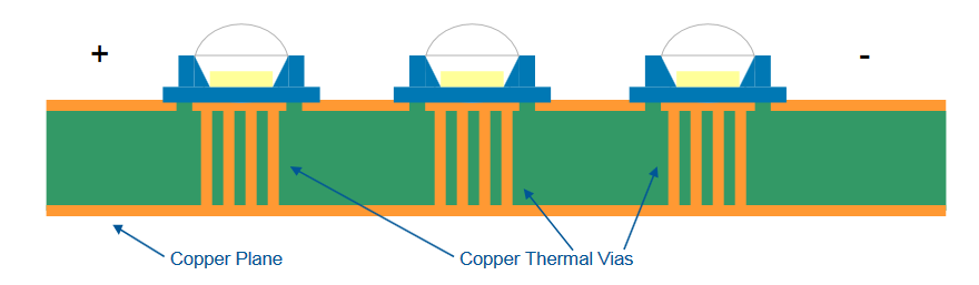
2. Thermal Management
In compact IoT designs, heat dissipation is a concern. Placing vias under components can sometimes trap heat, especially in high-power applications. Designers must incorporate thermal vias or heat sinks to manage temperatures effectively, ensuring device longevity.
3. Design Software Limitations
Not all PCB design tools fully support VIP layouts or provide accurate simulations for signal integrity in such configurations. Using advanced design software with VIP-specific features can streamline the process and reduce errors during prototyping.
Strategies for Using VIP in Small Footprint IoT Designs
To maximize the benefits of VIP while addressing its challenges, consider the following strategies tailored for IoT PCB design with a focus on wireless, low power, and cost-effective solutions.
1. Optimize Component Placement
Start by placing high-density components, such as microcontrollers or RF modules, in areas where VIP can have the most impact. For instance, in a wireless IoT sensor, position the Bluetooth chip to minimize trace lengths to the antenna, using VIP to connect directly to ground planes for better signal performance.
2. Use Microvias with VIP
Microvias, small-diameter vias often used in high-density interconnect (HDI) designs, pair well with VIP. They allow for finer pitch components and further reduce the PCB footprint. In a multi-layer IoT board, microvias can connect inner layers without occupying surface space, achieving up to 50% more routing density.
3. Prioritize Power Efficiency
For low power IoT devices, combine VIP with power management ICs (PMICs) placed strategically to minimize voltage drops. Use VIP to create direct connections to ground and power planes, reducing resistance and improving efficiency. This can help achieve power consumption as low as 1-2 μA in sleep mode for certain IoT applications.
4. Balance Cost and Performance
To keep designs cost-effective, evaluate whether VIP is necessary for all components or just critical high-density areas. For example, use VIP for BGA packages or RF sections, while sticking to traditional vias for less space-constrained parts. This hybrid approach can save on manufacturing costs without compromising core functionality.
Real-World Applications of VIP in IoT Devices
VIP technology is already making waves in various IoT applications. Here are a few examples of how it’s being used to achieve small PCB footprints and high performance.
Wearable Health Monitors: Devices like heart rate trackers need to be tiny yet reliable. VIP allows designers to pack sensors, processors, and wireless modules into a board smaller than 20 mm x 20 mm, all while maintaining low power usage for extended battery life.
Smart Home Sensors: Motion or temperature sensors for smart homes often operate on coin cell batteries. Using VIP, designers can reduce board size to fit into compact enclosures while ensuring efficient power distribution and strong wireless signals for Zigbee or Wi-Fi connectivity.
Industrial IoT Modules: In industrial settings, IoT devices monitor machinery in harsh environments. VIP helps create rugged, compact PCBs that withstand vibrations and temperature fluctuations, with shorter signal paths reducing noise in data transmission.
Best Practices for Designing with VIP in IoT
To ensure success when using VIP in your IoT PCB designs, follow these best practices:
- Collaborate Early with Manufacturers: Discuss VIP requirements with your PCB fabrication partner during the design phase to avoid costly redesigns. Ensure they can handle the precision needed for VIP and microvia drilling.
- Simulate Signal Integrity: Use simulation tools to analyze how VIP affects high-speed signals, especially for wireless IoT devices. Aim for impedance matching (typically 50 ohms for RF lines) to prevent signal reflections.
- Test Prototypes Thoroughly: Build and test multiple prototypes to identify potential issues like solder defects or thermal hotspots. For instance, measure temperature rises under load to ensure they stay within safe limits (e.g., below 85°C for most components).
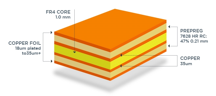
- Focus on Layer Stackup: Design your PCB stackup to balance signal, power, and ground layers. VIP works best in multi-layer boards (4-6 layers for IoT), allowing efficient routing without increasing board size.
Future Trends: VIP and IoT PCB Design
As IoT continues to grow, VIP technology will play an even larger role in enabling smaller, smarter devices. Emerging trends include the integration of VIP with flexible PCBs for wearable tech and the use of advanced materials to improve thermal performance in ultra-compact designs. Additionally, with 5G becoming mainstream, VIP will be critical for managing the high-frequency signals required for next-gen IoT connectivity.
At ALLPCB, we’re committed to staying at the forefront of these innovations, providing the tools and expertise to help you bring cutting-edge IoT products to market with minimal footprints and maximum efficiency.
Conclusion
Maximizing space in IoT devices is no longer just a goal—it’s a necessity. Via-in-Pad (VIP) technology offers a proven solution to reduce PCB size while supporting the demands of wireless connectivity, low power consumption, and cost-effective production. By understanding the benefits, challenges, and strategies for implementing VIP, you can create IoT designs that are not only smaller but also more reliable and efficient.
Whether you’re working on a wearable, a smart sensor, or an industrial IoT module, incorporating VIP into your PCB design can give you a competitive edge. Start exploring this technology today, and see how it can transform your next project into a compact powerhouse of innovation.