ALLPCB


If you're looking to improve the reliability of your PCB designs, mastering solder mask application is essential. Solder mask, a protective layer on printed circuit boards, prevents short circuits, protects copper traces, and ensures proper soldering. Key design rules include maintaining a solder mask clearance of 2-7 mils around pads, using a solder mask web of at least 4 mils between pads for stability, defining solder mask defined pads for precision, choosing appropriate solder mask colors for functionality, and carefully applying solder mask to vias to avoid issues like incomplete tenting. In this comprehensive guide, we'll dive deep into these topics, offering actionable tips and best practices to help you achieve flawless PCB manufacturing.
What Is Solder Mask and Why Does It Matter in PCB Design?
Solder mask, often called solder resist, is a thin polymer layer applied to a printed circuit board (PCB) to protect copper traces from oxidation, prevent unintended solder bridges during assembly, and insulate against environmental damage. Without a properly designed solder mask, your PCB risks short circuits, corrosion, and assembly errors, leading to costly rework or product failures.
For engineers and designers, understanding how to apply solder mask correctly is a critical skill. It directly impacts the board's durability, manufacturability, and performance. Whether you're working on a simple prototype or a complex multilayer board, following design rules ensures your PCB can withstand manufacturing processes and end-use conditions.

Key Solder Mask Design Rules for Reliable PCBs
Designing a solder mask layer requires attention to specific rules that ensure manufacturing accuracy and board reliability. Below, we break down the critical aspects, focusing on the long-tail keywords that matter most to PCB designers.
1. Solder Mask Clearance: Ensuring Precision Around Pads
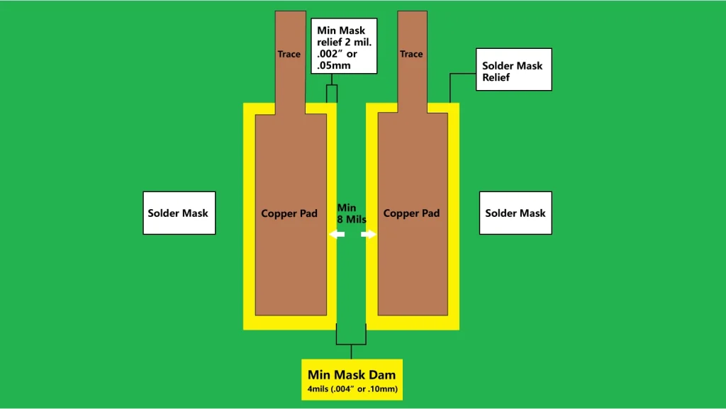
Solder mask clearance refers to the space between the edge of a copper pad and the surrounding solder mask layer. This clearance is vital to prevent misalignment during manufacturing, which could cover part of the pad and hinder soldering. A typical clearance value ranges from 2 to 7 mils (0.002 to 0.007 inches), depending on the PCB manufacturer's capabilities and the complexity of the design.
For standard designs, a clearance of 4 mils is often recommended as a safe middle ground. However, for high-density boards with fine-pitch components, you might need to reduce this to 2 mils, provided your manufacturer can handle the precision. Always check the fabrication house's design guidelines to avoid issues like solder mask slivers—thin, unwanted strips of mask that can peel off and cause defects.
Best Practice: Set clearance rules in your design software to automatically maintain consistent spacing. This reduces human error and ensures compliance with manufacturing tolerances.
2. Solder Mask Web: Maintaining Structural Integrity
The solder mask web is the narrow strip of solder mask material between two adjacent pads or features. A web that’s too thin can break or peel during manufacturing, leading to exposed copper and potential shorts. A minimum web width of 4 mils is generally advised to provide enough structural strength.
For high-reliability applications, such as aerospace or medical devices, consider increasing the web width to 6 mils or more if space allows. This added margin can prevent defects during thermal cycling or mechanical stress. On densely packed boards, balance the web width with clearance requirements to avoid compromising either.
Best Practice: Review your design for areas with closely spaced pads, especially near fine-pitch components like QFN packages, and adjust the web width to meet minimum standards.
3. Solder Mask Defined Pads: Precision for Soldering
Solder mask defined pads (SMD pads) are pads where the solder mask opening is smaller than the copper pad itself. This design creates a precise boundary for solder application, improving alignment during assembly and reducing the risk of solder bridging on small components.
In contrast, non-solder mask defined pads (NSMD) have a larger mask opening than the pad, which is often used for larger components or BGA packages to allow better solder flow. Choosing between SMD and NSMD depends on the component type and soldering process. For fine-pitch components, SMD pads with a 1-2 mil reduction in mask opening diameter compared to the pad size offer better control.
Best Practice: Use SMD pads for components with lead pitches below 0.5 mm to ensure precise solder placement, and document your choice in the design files to avoid confusion during fabrication.
4. Solder Mask Colors: Functionality Beyond Aesthetics
While solder mask colors like green, blue, red, black, and white might seem like a cosmetic choice, they serve practical purposes in PCB manufacturing and inspection. Green is the most common color due to its high contrast with copper and silkscreen markings, making visual inspection easier. It also has a well-established manufacturing process, ensuring consistency.
Other colors have specific uses:
- Blue: Often used for prototypes or to differentiate board versions during testing.
- Red: Provides good contrast and is sometimes used for branding purposes.
- Black: Absorbs heat, which can be useful or problematic depending on thermal requirements. It’s harder to inspect due to low contrast.
- White: Reflects light, often used in LED applications, but can show dirt easily.
Keep in mind that non-standard colors may increase manufacturing costs or lead times due to less common material availability. Additionally, darker colors like black can make automated optical inspection (AOI) more challenging.
Best Practice: Stick to green solder mask for standard projects to ensure compatibility with inspection processes, and reserve alternative colors for specific functional or branding needs.
5. Applying Solder Mask to Vias: Tenting, Plugging, or Leaving Open
Applying solder mask to vias is a critical decision that affects both manufacturing and performance. Vias are small holes that connect different layers of a PCB, and how you handle solder mask application to them can prevent or cause issues like solder wicking or contamination.
There are three main approaches to vias:
- Tenting: Covering the via with solder mask on both sides to protect it from solder and debris. This is common for vias not used as test points. Ensure the mask fully covers the via to avoid incomplete tenting, which can trap contaminants. A minimum via diameter of 0.3 mm is often required for reliable tenting.
- Plugging: Filling the via with a non-conductive material before applying solder mask. This is used for via-in-pad designs to prevent solder from flowing into the via during reflow. Plugging adds cost but is essential for high-density designs.
- Leaving Open: No solder mask coverage, often used for test points or thermal vias. Be cautious, as open vias near pads can lead to solder wicking, reducing the solder available for component attachment.
Best Practice: Default to tenting vias unless they serve a specific purpose like testing or heat dissipation. Clearly specify via treatment in your design files to avoid miscommunication with the manufacturer.
Common Solder Mask Mistakes and How to Avoid Them
Even with the best design rules, errors can creep into solder mask application if you're not careful. Here are some frequent mistakes and tips to prevent them:
- Insufficient Clearance: Too small a clearance can lead to mask covering part of the pad, causing soldering defects. Always double-check clearance values against manufacturer specs.
- Thin Solder Mask Webs: Webs below 4 mils risk breaking during fabrication. Use design rule checks (DRC) in your software to flag potential issues.
- Incomplete Via Tenting: If the solder mask doesn’t fully cover a via, contaminants can enter. Specify tenting requirements and verify with a pre-production review.
- Misalignment: Solder mask misalignment can expose copper or cover pads. Provide accurate Gerber files and include a registration layer for alignment during fabrication.
Advanced Tips for Solder Mask Design in High-Reliability Applications
For industries like automotive, aerospace, or medical, where PCB reliability is non-negotiable, consider these advanced practices:
- Increase solder mask thickness to 0.8-1.2 mils (standard is 0.5-0.8 mils) for added protection against harsh environments.
- Use liquid photoimageable solder mask (LPSM) for finer resolution compared to traditional epoxy masks, especially on high-density boards.
- Perform a design for manufacturability (DFM) check to simulate potential issues like mask slivers or misalignment before sending files to production.
Conclusion: Elevate Your PCB Designs with Proper Solder Mask Practices
Mastering solder mask design is a cornerstone of reliable PCB manufacturing. By adhering to key rules like maintaining proper solder mask clearance, ensuring adequate solder mask web width, using solder mask defined pads for precision, selecting functional solder mask colors, and carefully applying solder mask to vias, you can significantly reduce manufacturing defects and improve board performance.
Take the time to review your designs against these best practices, and always communicate clearly with your fabrication partner to align on specifications. With these strategies in place, you'll be well-equipped to produce high-quality PCBs that meet both functional and reliability standards.