 ALLPCB


Introduction
Laser PCB etching represents a significant evolution in printed circuit board manufacturing, shifting from traditional chemical methods to advanced laser-based techniques. This process utilizes focused laser beams to selectively remove material from copper-clad substrates, enabling the creation of intricate circuit patterns with exceptional control. For electric engineers working on high-density designs or rapid iterations, laser etching offers a pathway to improved precision and reduced lead times in production workflows. Factory environments increasingly adopt this method to meet demands for finer features in modern electronics. As board complexity grows, understanding laser PCB etching becomes essential for optimizing manufacturing outcomes. This article explores the process, comparisons, advantages, and practical applications tailored to engineering needs.
Understanding the Laser PCB Etching Process
The laser PCB etching process begins with preparing a copper-clad laminate, typically FR-4 material, where the laser targets specific areas for material removal. In direct ablation methods, high-powered fiber or UV lasers vaporize copper layers without additional chemicals, creating clean traces through thermal or photochemical interactions. Alternatively, hybrid approaches use the laser to ablate a photosensitive resist or painted mask, exposing copper for subsequent chemical etching. Engineers control parameters like wavelength, pulse duration, and power density to achieve desired depth and width in the etched features. This non-contact nature minimizes mechanical stress on the substrate during operation. Overall, the process aligns with factory standards for consistent pattern transfer in multilayer boards.
Laser systems employ galvo scanners for precise beam steering across the board surface, ensuring uniform etching even on irregular topographies. Post-etching, cleaning steps remove residues, preparing the board for plating or solder mask application. Quality checks verify trace integrity against specifications like line width and spacing. In production lines, automation integrates laser etching with imaging systems for real-time alignment. This workflow supports both prototyping and small-batch runs effectively.
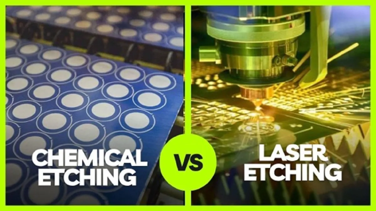
Laser Etching vs Chemical Etching: Key Differences
Chemical etching submerges the entire board in etchants like ferric chloride, dissolving unprotected copper isotropically and often leading to undercuts at trace edges. Laser etching, by contrast, delivers energy only to targeted areas, producing vertical sidewalls and sharper definitions without lateral material loss. Factories favor chemical methods for high-volume production due to their scalability, but laser excels in applications requiring tight tolerances. Chemical processes generate hazardous waste and require extensive rinsing, while laser direct ablation reduces environmental impact through dry processing. Engineers note that laser methods handle varying copper thicknesses more reliably without over-etching risks.
In terms of throughput, laser etching accelerates prototyping cycles, completing a board in minutes compared to hours for chemical setups. Chemical etching demands precise control of etchant concentration and temperature to avoid inconsistencies, whereas laser parameters adjust dynamically via software. For multilayer boards, laser integration with via drilling enhances overall efficiency. Compliance with IPC-A-600K acceptability criteria becomes straightforward with laser's repeatability. Ultimately, the choice depends on volume, feature size, and facility capabilities.
- Precision - Laser: High with vertical walls and micron-level accuracy; Chemical: Moderate, prone to undercuts.
- Speed - Laser: Fast for prototypes and small batches; Chemical: Slower, batch-oriented.
- Waste - Laser: Minimal, dry process; Chemical: Produces chemical sludge, rinsing required.
- Flexibility - Laser: Easy digital design changes; Chemical: Requires fixed tooling and masks.
- Cost - Laser: Higher initial setup; Chemical: Lower per-unit cost for mass production.
Advantages of Laser PCB Etching
One primary advantage of laser PCB etching lies in its superior precision, enabling features down to fine resolutions suitable for high-frequency circuits. Engineers benefit from reduced variability, as the laser beam focuses energy precisely, avoiding the diffusion issues common in wet processes. This method supports complex geometries, such as stepped trenches or blind vias, integrated into a single setup. Factory-driven insights highlight how laser etching minimizes defects like bridging or shorts through controlled ablation depths. Additionally, it accommodates diverse substrates, including flex and rigid-flex materials, expanding design possibilities.
Laser PCB etching accelerates iteration cycles, crucial for design validation phases. Unlike chemical etching, which requires mask preparation and development, laser processes patterns directly from digital files, slashing setup times. This digital workflow integrates seamlessly with CAD software, allowing on-the-fly adjustments. Environmental benefits include lower chemical usage, aligning with sustainability goals in manufacturing. For electric engineers, the non-contact process preserves substrate integrity, reducing warpage risks during handling.
Another key benefit is scalability from prototypes to low-volume production without retooling. Laser systems maintain consistency across runs, supporting IPC-6012E qualification for rigid boards. Cost savings emerge over time through reduced waste and faster turnaround. Engineers report improved yield rates, particularly for dense interconnects.
Laser PCB Prototyping: Speed and Flexibility
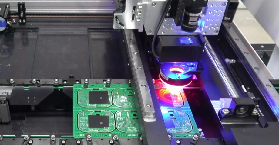
Laser PCB prototyping transforms engineering workflows by enabling in-house fabrication of functional boards within hours. Engineers load Gerber files into laser control software, which translates designs into etching paths with fiducial alignment for accuracy. This rapid method suits proof-of-concept testing, where quick revisions address signal integrity or thermal issues. Factories leverage laser prototyping to bridge the gap between design and full production, minimizing external dependencies. The process handles single- or double-sided boards efficiently, often completing etching, cutting, and drilling in one station.
Flexibility shines in customizing prototypes for specific applications, such as RF modules or sensors requiring precise impedance control. Laser etching avoids the minimum order quantities of traditional services, ideal for low-volume R&D. Post-prototype, boards transition smoothly to volume manufacturing with verified patterns. Engineers appreciate the ability to prototype on varied copper weights without process tweaks.
In practice, laser prototyping reduces time-to-market, fostering innovation cycles. Integration with desmear and plating steps ensures prototypes mirror production boards. This approach empowers teams to validate assemblies early.
Achieving Precision PCB Etching: Best Practices
To maximize precision PCB etching, engineers start with substrate selection, opting for stable laminates to counteract thermal effects from laser energy. Calibrating laser parameters, including spot size and repetition rate, proves critical for uniform ablation across the panel. Factory protocols include pre-scan alignment using optical fiducials to compensate for board shifts. Implementing assist gases, like nitrogen, clears debris and prevents oxidation during etching. Regular maintenance of optics maintains beam quality, essential for consistent results.
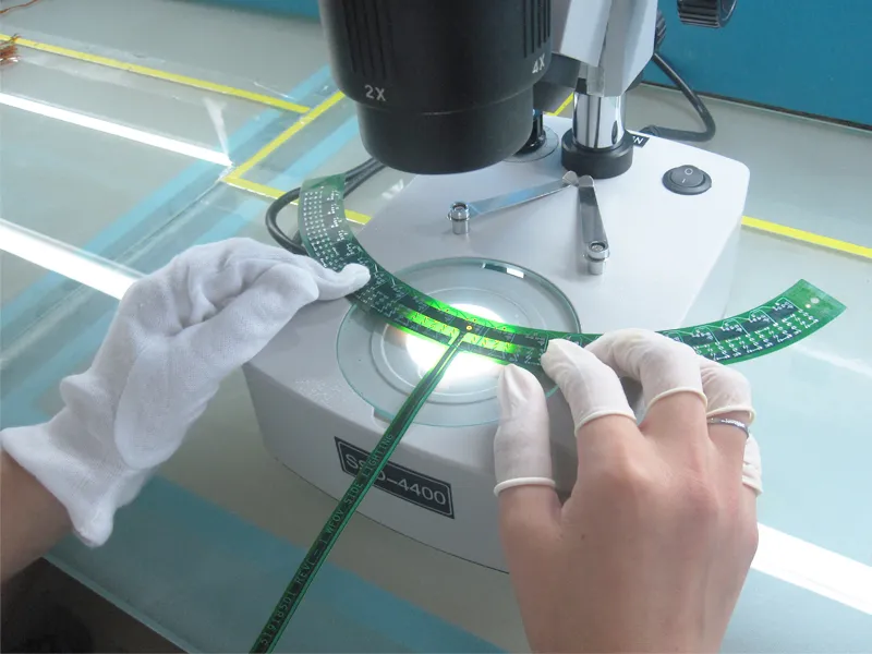
Process monitoring via inline imaging detects anomalies, allowing real-time corrections. For multilayer applications, sequencing laser passes layer-by-layer ensures depth control. Adhering to J-STD-020E for handling sensitivity during prototyping prevents moisture-related defects. Post-etch inspection verifies compliance with design rules, such as annular ring widths.
Best practices extend to workflow integration, combining etching with routing for complete panels. Training operators on software optimization enhances throughput. These steps elevate laser etching from prototyping tool to production staple.
Conclusion
Laser PCB etching redefines circuit board manufacturing through its blend of precision, speed, and versatility, particularly appealing to electric engineers tackling complex designs. From direct ablation to hybrid methods, it outperforms chemical etching in prototyping and fine-feature production while aligning with industry standards. Advantages like minimal waste and design flexibility position it as a factory essential for future electronics. By adopting best practices, teams achieve reliable outcomes compliant with IPC specifications. As demands for denser boards grow, laser etching will play a pivotal role in efficient, high-quality manufacturing.
FAQs
Q1: What is the laser PCB etching process?
A1: The laser PCB etching process uses a focused beam to ablate copper or remove resist from clad boards, creating circuit patterns. Direct methods vaporize material thermally, while hybrids prepare for chemical steps. Engineers control parameters for precision, making it ideal for prototypes. This dry or semi-dry approach reduces handling compared to full immersion etching. Factories integrate it for rapid iterations.
Q2: How does laser etching compare to chemical etching for PCBs?
A2: Laser etching offers higher precision with vertical walls, avoiding undercuts common in chemical methods. It processes boards faster for low volumes and generates less waste. Chemical etching suits mass production but requires etchants and rinsing. Laser excels in flexibility for design changes. Both ensure quality, but laser aligns better with prototyping needs.
Q3: What are the main advantages of laser PCB etching?
A3: Advantages of laser PCB etching include micron-level accuracy, quick turnaround, and non-contact processing that preserves board integrity. It supports complex traces without chemicals in direct ablation. Engineers gain from digital control and reduced defects. Factory use lowers environmental impact. Overall, it boosts prototyping efficiency.
Q4: Why is laser PCB prototyping preferred for precision etching?
A4: Laser PCB prototyping delivers precision etching through adjustable beams and fiducial alignment, enabling fine features rapidly. It handles high-density designs without masks. Engineers prototype in-house, cutting lead times. Compliance with standards like IPC-A-600K verifies quality. This method accelerates validation for electric applications.
References
IPC-6012E - Qualification and Performance Specification for Rigid Printed Boards. IPC, 2017
IPC-A-600K - Acceptability of Printed Boards. IPC, 2020
J-STD-020E - Moisture/Reflow Sensitivity Classification. JEDEC, 2014


