 ALLPCB


Introduction
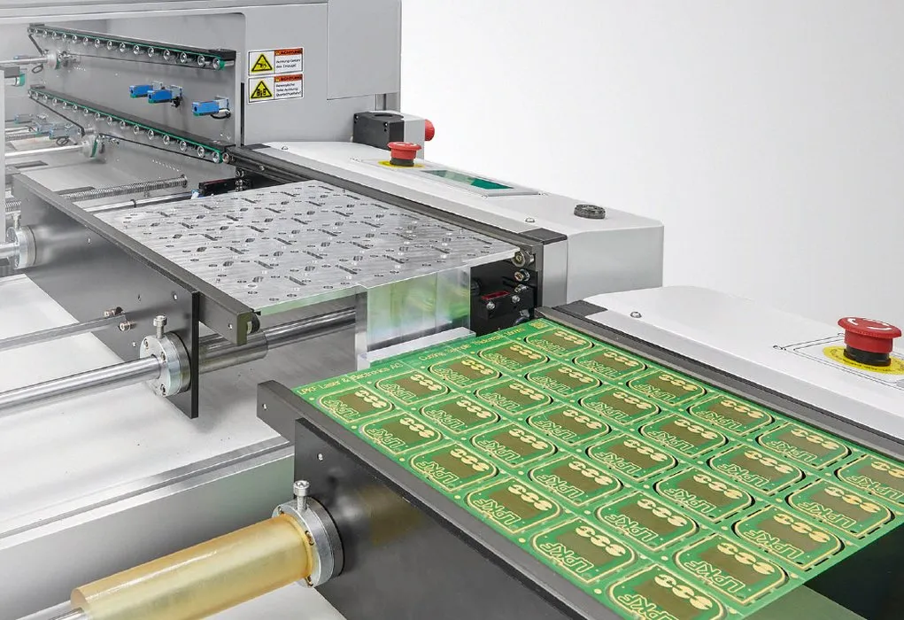
In modern electronics manufacturing, printed circuit boards (PCBs) with intricate designs demand separation methods that preserve integrity and functionality. Laser depaneling machines have emerged as a key solution for singulating PCBs from production panels, particularly when handling high-density interconnects and fine-pitch components. This process uses focused laser beams to ablate material along predefined paths, enabling ultra-precise cuts without physical contact. Engineers face challenges with traditional mechanical methods that introduce stress, burrs, and particles, potentially compromising board reliability. Laser depaneling addresses these issues by offering laser depaneling precision that supports miniaturization trends in consumer electronics, automotive systems, and medical devices. As PCB complexity increases, understanding this technology becomes essential for optimizing production yields and quality.
What Is Laser Depaneling and Why It Matters
Laser depaneling involves directing a high-energy laser beam to vaporize or ablate the PCB substrate along scored or routed paths, separating individual boards cleanly from the panel. Unlike mechanical routing or punching, which rely on tools that generate vibration and debris, laser systems operate in a non-contact manner. This method excels in environments requiring laser depaneling precision, where tolerances must stay within micrometers to avoid damaging nearby components. Its relevance grows with the shift toward complex PCB shapes, such as those with curved edges, tight radii, or irregular outlines that mechanical tools struggle to produce consistently.
The process matters because modern PCBs often integrate sensitive surface-mount devices, fine traces, and multilayer stacks that cannot tolerate mechanical stress. Poor depaneling can lead to microcracks, delamination, or component failures during subsequent assembly or operation. Laser depaneling minimizes these risks, aligning with industry demands for higher yields in high-mix, low-volume production. For electric engineers designing boards for reliability, selecting the right depaneling method directly impacts compliance with quality benchmarks like IPC-A-600 acceptability criteria. Ultimately, it enables denser panel utilization and faster design iterations without custom tooling.
Technical Principles of Laser Depaneling
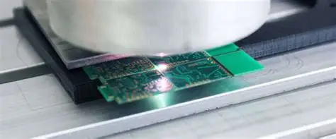
Laser depaneling relies on the interaction of a focused beam with the PCB material, typically FR-4 epoxy resin reinforced with glass fibers. Common wavelengths include ultraviolet (UV) at 355 nm for minimal heat-affected zones (HAZ) or CO2 at longer wavelengths for thicker substrates. The beam's spot size, pulse duration, and repetition rate determine the kerf width, often limited to a few hundred micrometers, allowing cuts near active features.Galvanometer scanners or motion stages guide the beam along vectorized paths generated from Gerber files, ensuring positional accuracy better than 25 micrometers in advanced systems.
Key mechanisms include ablation, where photons break molecular bonds, ejecting material as vapor or plasma without melting. This produces clean edges free of burrs or recast layers common in thermal processes. Process parameters like fluence (energy per unit area) and scan speed must balance cut depth with HAZ control, critical for multilayer boards. Vision systems often calibrate fiducials to compensate for panel warpage, maintaining tolerances during extended runs. Engineers must consider substrate thickness, typically up to 2 mm, and copper cladding, as lasers selectively remove dielectric while minimizing metal interaction.
For rigid-flex hybrids, dual-wavelength systems may combine UV for precision and infrared for penetration. Cooling via assist gas or vacuum extraction prevents thermal buildup. These principles enable laser depaneling precision that surpasses mechanical alternatives, supporting feature sizes down to 50 micrometers from cut lines.
Laser Depaneling Benefits Over Traditional Methods
Laser depaneling offers several advantages rooted in its non-contact nature. Mechanical routing uses spinning bits that create wide kerfs (1.5 to 3 mm) and generate dust, risking contamination of optical components or ESD-sensitive parts. In contrast, lasers produce particle-free environments, ideal for cleanroom operations. Stress-free separation prevents warping or cracking in thin boards, preserving electrical performance.
Another benefit is flexibility for high-mix production. Without dedicated tooling, setups change via software in minutes, unlike routers requiring bit swaps or punches needing dies. This reduces lead times for prototypes and custom runs. Laser depaneling benefits also include material savings through tighter tab spacings, as small as 100 micrometers between boards. Yield improvements stem from consistent edge quality, meeting IPC-6012 performance specifications for rigid boards.
Compared to V-scoring or breakaway tabs, lasers handle arbitrary geometries without predefined straight lines. Dust and burr removal post-processing is eliminated, streamlining workflows. For electric engineers, these factors translate to lower defect rates and reliable field performance in vibration-prone applications.
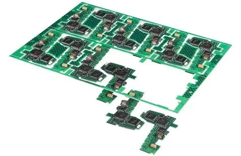
Cutting Complex PCB Shapes with Laser Depaneling
Complex PCB shapes, such as those with non-rectangular outlines, cutouts, or proximity to gold fingers, challenge conventional depaneling. Laser systems excel here by following arbitrary contours programmed from design files, achieving smooth radii down to 0.2 mm. Mechanical routers often require wider paths to avoid bit breakage, wasting panel real estate. Lasers maintain laser depaneling precision across curves, minimizing overcut.
In practice, engineers vectorize the singulation path to optimize beam overlap and direction changes, reducing heat accumulation at corners. For high-frequency boards, edge roughness below 5 micrometers ensures signal integrity by avoiding reflections. Flexible circuits benefit from tension-free cuts, preventing delamination in polyimide layers. This capability supports innovative designs like wearables or IoT modules with ergonomic forms.
Panel layout optimization is crucial: fiducial marks aid alignment, and mouse bites can hybridize with laser for straight sections. Testing cut paths on scrap panels verifies tolerances before production. Overall, laser depaneling transforms cutting complex PCB shapes from a bottleneck into a strength.
Practical Solutions and Best Practices
Implementing laser depaneling requires structured process control. Start with design rules: maintain at least 100 micrometers from laser paths to components or traces. Simulate paths using CAM software to predict HAZ and optimize parameters. Vacuum fixturing secures panels without clamps that could distort thin laminates.
Best practices include inline vision for real-time adjustments and process monitoring via power meters. Calibrate for material variations, as copper density affects ablation rates. For multilayer stacks, sequential passes ensure complete penetration without breakthrough damage. Post-cut inspection per IPC-A-600 verifies edge quality classes.
Hybrid approaches pair lasers with routing for thick sections, balancing speed and precision. Operator training on parameter tuning prevents common issues like incomplete cuts. Maintenance schedules for optics and exhaust systems sustain uptime above 90 percent.
Cost Considerations for Laser Depaneling Machines
The cost of laser depaneling machines involves upfront investment, operational expenses, and long-term savings. Initial purchases reflect system capabilities, with entry-level units for prototypes differing from high-throughput inline models. Factors like laser power, automation, and enclosure size influence pricing, often offset by no tooling costs versus mechanical dies running thousands per design.
Running costs include power, assist gases, and consumables like filters, generally lower than router bit replacements. Market growth indicates economies of scale, with global equipment values rising steadily. Payback periods shorten in high-mix scenarios through reduced scrap and labor. Engineers evaluate total cost of ownership, factoring yield gains meeting IPC-6012 standards.
Conclusion
Laser depaneling machines deliver ultra-precision cuts essential for complex PCB designs, outperforming mechanical methods in accuracy and versatility. Key strengths lie in stress-free operation, narrow kerfs, and adaptability to intricate shapes, enhancing manufacturing efficiency. Electric engineers benefit from reliable processes that uphold quality standards while supporting innovation. As demands for miniaturization intensify, integrating laser depaneling optimizes production pipelines. Adopting best practices ensures maximum return on investment.
FAQs
Q1: What defines laser depaneling precision in PCB manufacturing?
A1: Laser depaneling precision refers to the ability to achieve narrow kerf widths, often a few hundred micrometers, and positional accuracies under 25 micrometers. This enables cuts near fine-pitch components without damage, surpassing mechanical tolerances. Vision-guided systems and ablation control minimize variations, ensuring consistent edge quality for high-reliability applications.
Q2: How does laser depaneling benefit cutting complex PCB shapes?
A2: Laser depaneling benefits cutting complex PCB shapes by following arbitrary contours without tooling, producing burr-free edges and zero mechanical stress. It supports tight radii and irregular outlines, maximizing panel utilization. Software-defined paths allow rapid changes, ideal for prototypes and custom designs in electric engineering projects.
Q3: What are the main laser depaneling benefits compared to routing?
A3: Laser depaneling benefits include particle-free, stress-free separation with superior precision and flexibility. Unlike routing, it avoids vibration-induced microcracks and wide kerfs, reducing waste. No custom tools lower setup costs for high-mix runs, improving yields and cleanroom compatibility.
Q4: What factors affect the cost of laser depaneling machines?
A4: The cost of laser depaneling machines depends on power, automation, and throughput capacity. Higher initial outlay is balanced by zero tooling expenses and lower maintenance than mechanical systems. Operational savings from reduced scrap and faster changeovers justify investment in demanding production environments.
References
IPC-6012E — Qualification and Performance Specification for Rigid Printed Boards. IPC, 2017
IPC-A-600K — Acceptability of Printed Boards. IPC, 2020
IPC-2221 — Generic Standard on Printed Board Design. IPC, 2012


