ALLPCB


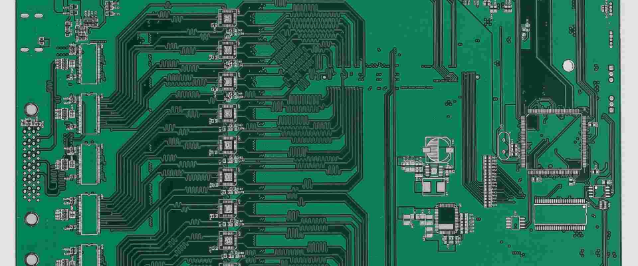
High-layer-count printed circuit boards have become essential in advanced electronic systems where dense routing, multiple power domains, and high-speed signaling must coexist within a compact footprint. Engineers designing these boards face increasing pressure to maintain signal integrity across dozens of layers while meeting strict impedance targets and minimizing electromagnetic interference. A well-planned PCB stackup directly influences trace impedance, crosstalk, return-path continuity, and overall system reliability. Effective stackup design therefore serves as a foundational step rather than an afterthought in the development process.
Why High-Layer-Count PCB Stackup Design Matters
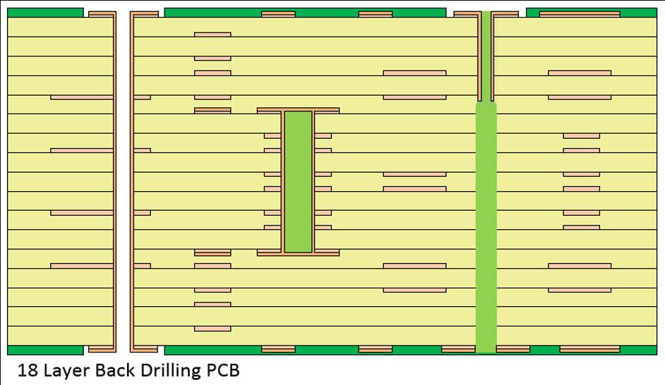
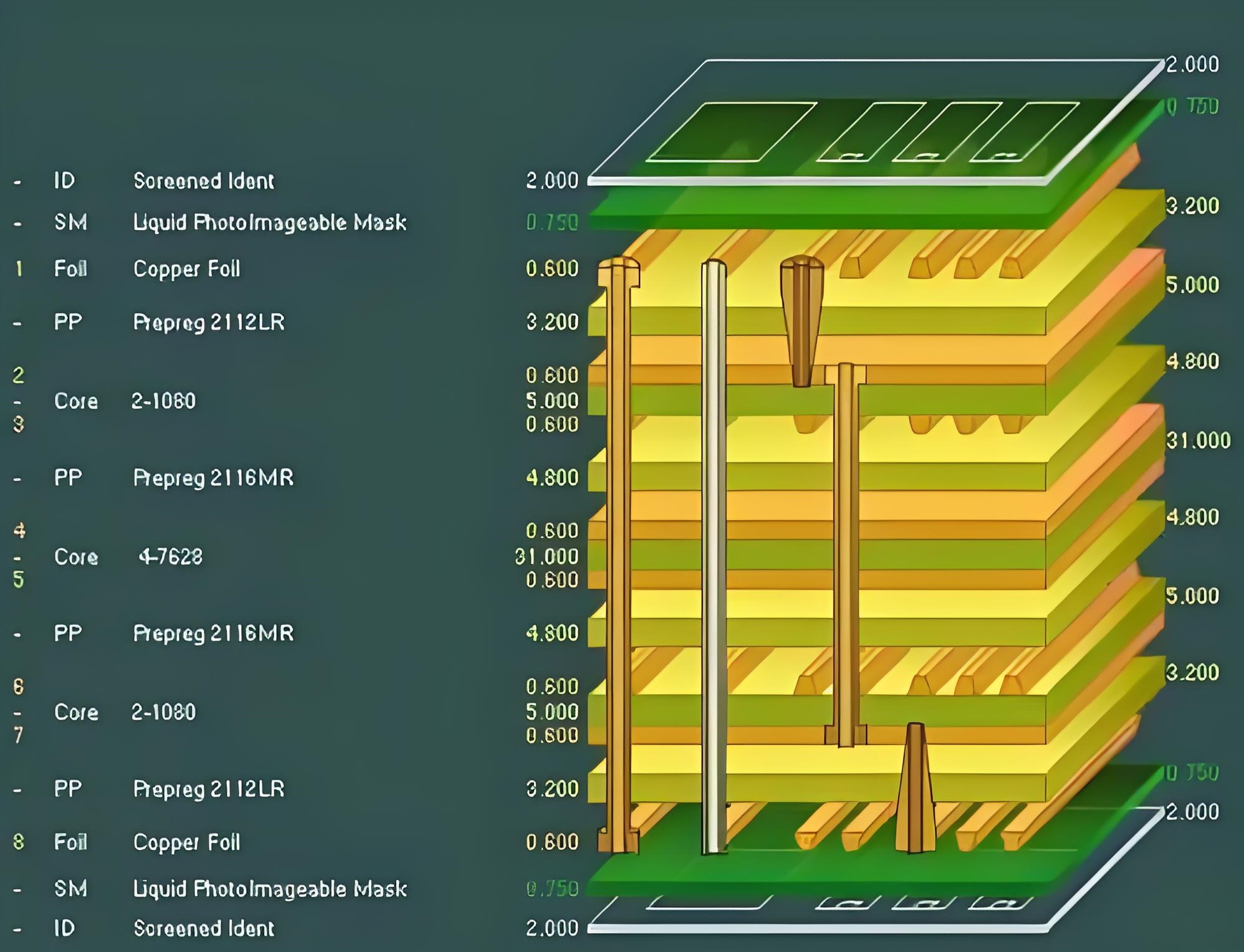
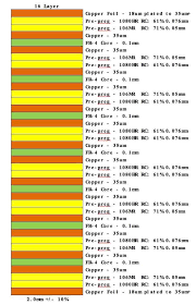
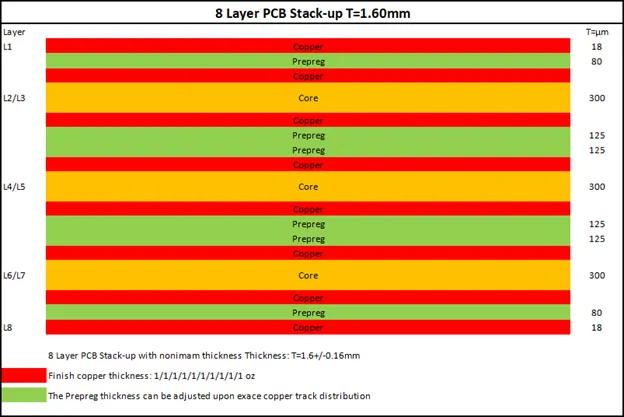
A PCB stackup defines the arrangement of copper layers, dielectric materials, and core or prepreg thicknesses that together form the board. In high-layer-count designs, typically exceeding eight layers, the stackup must balance electrical performance with mechanical stability and manufacturability. Poor stackup choices can lead to impedance mismatches that degrade signal quality or create excessive crosstalk between adjacent traces. Industry standards such as IPC-6012E establish qualification requirements that guide acceptable layer registration, dielectric thickness tolerances, and overall board performance for rigid printed boards. These considerations become especially critical in applications involving high-speed serial links, memory interfaces, or mixed-signal circuits where even small deviations can cause bit errors or timing violations.
Technical Principles of Signal Integrity in Multilayer Stackups
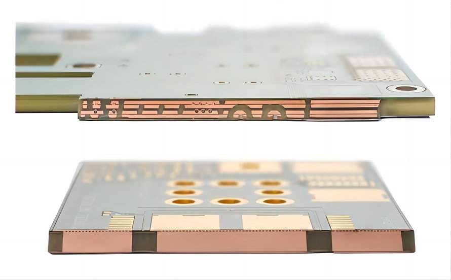
Signal integrity in high-layer-count boards depends on precise control of characteristic impedance, which is determined by trace geometry, dielectric constant, and the proximity of reference planes. When signals travel on inner layers, they require adjacent ground or power planes to provide low-inductance return paths; any interruption in these planes forces current to take longer routes and increases loop inductance. Crosstalk arises primarily from capacitive and inductive coupling between parallel traces, and its severity grows with higher layer counts because more signals share limited board real estate. Dielectric materials must exhibit stable electrical properties across frequency and temperature ranges to keep propagation delay consistent. Vias introduce additional discontinuities through their stubs and barrel capacitance, making via placement and back-drilling decisions integral to the overall stackup strategy.
Symmetric layer arrangements help control warpage during thermal cycling by balancing copper distribution and resin content on both sides of the board center. Reference planes should be placed immediately adjacent to high-speed signal layers to minimize the distance current must travel to complete its loop. Differential pairs require matched trace widths and spacing, along with consistent dielectric thickness above and below the pair, to achieve the target differential impedance. Power distribution networks also benefit from dedicated planes that reduce voltage ripple and provide shielding between noisy digital sections and sensitive analog circuits.
Best Practices for PCB Stackup Design and Impedance Control
Begin the stackup process by defining the required impedance values for single-ended and differential signals early in the design cycle. Work with fabricators to select dielectric materials whose dielectric constants and loss tangents meet the frequency requirements of the application. Maintain consistent trace widths and spacings across layers by using the same dielectric thickness for all signal layers that carry similar impedance targets. Place ground planes directly above and below critical signal layers to establish controlled impedance environments and reduce crosstalk. Route high-speed signals on layers with the fewest via transitions possible, and consider back-drilling or blind/buried vias when stub lengths would otherwise degrade signal quality.
Power planes should be positioned to provide both low-impedance distribution and effective shielding. Avoid splitting reference planes under high-speed traces, because splits force return currents to detour and create impedance discontinuities. Document the complete stackup, including copper weights, dielectric types, and finished thicknesses, so that simulation tools can accurately predict performance before layout begins. Review the stackup against IPC-A-600K acceptability criteria to confirm that layer-to-layer registration and dielectric uniformity will remain within acceptable limits after lamination.
Practical Implementation Considerations
Engineers should simulate the proposed stackup using electromagnetic field solvers to verify impedance targets and identify potential resonances before committing to fabrication. Thermal management also influences material selection, because high-layer-count boards can trap heat if copper distribution is uneven. Sequential lamination processes allow complex via structures but add cost and require careful planning of layer build-up order. Test coupons fabricated alongside production panels enable post-production verification of impedance and dielectric properties, confirming that the realized board matches the design intent.
Conclusion
High-layer-count PCB stackup design requires systematic attention to impedance control, reference-plane integrity, and material properties to preserve signal integrity. Structured engineering decisions made early in the project reduce the need for costly respins and improve overall system reliability. By following established qualification and acceptability guidelines, design teams can achieve repeatable results across multiple production lots.
FAQs
Q1: What defines a high-layer-count PCB stackup?
A1: A high-layer-count PCB stackup generally refers to boards with eight or more conductive layers arranged to support dense routing and multiple signal domains. Proper arrangement of signal, ground, and power layers helps maintain consistent impedance and minimizes crosstalk. Engineers must balance electrical requirements with mechanical stability during the design phase.
Q2: How does PCB stackup design affect signal integrity PCB performance?
A2: PCB stackup design determines the proximity of traces to reference planes, which directly controls characteristic impedance and return-path inductance. Incorrect layer ordering can increase crosstalk or create discontinuities that degrade high-speed signals. Careful planning of dielectric thicknesses and copper weights supports reliable transmission of data across the board.
Q3: Why is impedance control PCB important in multilayer designs?
A3: Impedance control PCB ensures that trace geometry and surrounding dielectrics produce the target impedance values required by drivers and receivers. Deviations cause reflections that reduce signal amplitude and increase timing uncertainty. Consistent impedance across all relevant layers supports clean data transmission in high-speed applications.
Q4: What role do industry standards play in high-layer-count PCB stackup?
A4: Industry standards such as IPC-6012E provide qualification requirements that verify layer registration, dielectric thickness, and overall board integrity after fabrication. These guidelines help ensure that the finished product meets electrical and mechanical specifications. Compliance supports consistent performance across production runs.
References
IPC-6012E — Qualification and Performance Specification for Rigid Printed Boards. IPC, 2017
IPC-A-600K — Acceptability of Printed Boards. IPC, 2020