 ALLPCB


Introduction
Heavy copper PCBs play a critical role in modern automotive power electronics, where high current demands require robust substrates to handle power conversion efficiently. These boards feature copper layers significantly thicker than standard 1-ounce foils, enabling them to support the intense electrical loads in electric vehicles and hybrid systems. As automotive systems shift toward higher power densities, automotive PCB heavy copper designs become essential for components like inverters and DC-DC converters. This approach enhances current carrying capacity while minimizing losses and heat generation. Engineers designing power PCB layouts must prioritize these thick copper PCB solutions to meet performance targets in demanding environments. The following sections explore the principles, applications, and best practices for integrating heavy copper into automotive power electronics.
What Are Heavy Copper PCBs and Why Do They Matter in Automotive Power Electronics?
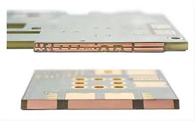
Heavy copper PCBs are printed circuit boards with copper cladding exceeding 2 ounces per square foot, often ranging up to 20 ounces or more in specialized designs. This thickness provides superior current handling compared to standard PCBs, making them ideal for high current PCB design in power-intensive applications. In automotive power electronics, components such as inverters and DC-DC converters must manage hundreds of amps under continuous operation, where thin copper would lead to excessive resistance and thermal runaway. Thick copper PCB constructions reduce voltage drops and allow for more compact layouts, which is crucial in space-constrained vehicle modules. Reliability improves as these boards withstand vibration, thermal cycling, and humidity typical in automotive settings. For electric engineers, understanding heavy copper's role ensures optimized power PCB design that aligns with vehicle electrification trends.
The relevance stems from the evolution of automotive systems toward electrification, demanding boards that support megawatt-scale powertrains without failure. Standard PCBs suffice for signal processing, but power sections require heavy copper to prevent hotspots and maintain efficiency. This technology directly impacts system costs by enabling fewer parallel traces and smaller heatsinks. Automotive OEMs specify these boards to meet stringent safety and performance criteria, influencing the entire supply chain.
Technical Principles Behind Enhanced Current Carrying Capacity
Current carrying capacity in PCBs depends on copper thickness, trace geometry, and operating temperature, with thicker foils inherently supporting higher amperages due to lower resistance. According to IPC-2152 guidelines, external traces on heavy copper layers can carry significantly more current per unit width than standard foils, as resistance scales inversely with cross-sectional area. For instance, doubling copper thickness halves the resistance for a given trace width, allowing sustained high currents without exceeding safe temperature rises. Skin effect becomes relevant at higher frequencies, but in automotive power electronics operating below 100 kHz, DC-like behavior dominates, favoring thick copper for uniform current distribution.
Thermal management is intertwined, as heavy copper acts as both conductor and heat spreader, dissipating Joule heating more effectively across the board. Cross-sectional area determines the I2R losses, so automotive PCB heavy copper designs leverage this to keep junction temperatures within limits. Multilayer stacks with heavy copper inner layers further enhance vertical heat transfer to thermal vias and planes. Engineers must model these effects using finite element analysis to predict hotspots accurately. The result is a power PCB design capable of 50% higher currents than equivalents with thin copper, without proportional size increases.
Electromigration and intermetallic growth pose risks under high currents, but heavy copper mitigates these by reducing current density. Voids form less readily in thicker foils, extending mean time between failures. Automotive environments amplify these stresses with rapid power cycling, so material purity and grain structure in the copper plating become key factors.
Key Applications in Automotive Power Electronics
Automotive inverter PCBs represent a prime use case for heavy copper, where three-phase power conversion from battery to motor demands robust current paths. Inverters handle peak currents exceeding 1000 A during acceleration, requiring thick copper bus bars integrated into the PCB for low-inductance switching. Heavy copper layers support the IGBT modules and gate drivers, minimizing stray inductance that could cause voltage overshoots. This design choice enhances efficiency in traction inverters, critical for range extension in electric vehicles. Troubleshooting common issues like trace delamination often traces back to insufficient copper weight, underscoring the need for verified heavy copper implementations.
Similarly, automotive DC-DC converter PCBs benefit from high current PCB design principles, converting high-voltage battery power to low-voltage auxiliaries. Bidirectional converters in modern vehicles manage 400 V to 12 V at high power levels, where thick copper PCB traces prevent efficiency drops from IR losses. Power stages with synchronous rectification rely on low-resistance paths to handle RMS currents continuously. Integrating heavy copper allows designers to embed current sensors directly on the board, improving control loop accuracy. Field failures in these converters often stem from underrated copper thickness, leading to overheating during regenerative braking.
Power distribution modules also employ heavy copper for fusing and shunting, ensuring safe current limiting without bulky wiring harnesses. These applications collectively drive the adoption of automotive PCB heavy copper across the powertrain.
Design Best Practices for High Current PCB Implementation
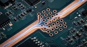
Start with stackup planning, allocating heavy copper to power planes and traces while balancing with thinner signal layers for control circuitry. Use wider traces or multiple parallel paths calculated per IPC-2152 to achieve target ampacity, incorporating temperature rise margins for automotive derating. Via stitching enhances current sharing in multilayer power PCB designs, preventing localized heating. Simulate electromagnetic compatibility early, as thick copper can alter impedance profiles.
Material selection focuses on high-Tg laminates compatible with heavy copper plating, ensuring adhesion under thermal stress. Sequential lamination builds heavy copper multilayers without warpage, adhering to IPC-6012 qualification for rigid boards. Solder mask over heavy copper requires thicker application to avoid cracking during flexing.
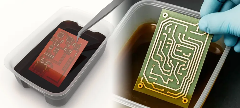
Fabrication tolerances tighten for thick copper PCB etching, where differential etching rates demand panel plating over pattern plating. Post-etch planarization maintains flatness for assembly. In assembly, reflow profiles adjust for heavier thermal mass, following J-STD-001 requirements to avoid cold joints.
Testing verifies current capacity through thermal imaging and resistance measurements under load. Accelerated life testing simulates automotive cycles, confirming reliability.
Troubleshooting Common Challenges in Heavy Copper Automotive PCBs
Warpage emerges as a frequent issue during lamination of thick copper layers, exacerbated by CTE mismatches between copper and FR-4. Mitigate by symmetric stackups and constrained processing fixtures. Plating voids in heavy copper vias lead to high resistance; inspect with cross-sectioning and use filled vias for power paths.
Overheating in high current zones signals inadequate cooling; add embedded heat pipes or direct liquid cooling interfaces. Signal integrity degrades near power traces due to crosstalk, resolved by ground shielding and length matching.
Assembly defects like tombstoning increase with thermal mass differences; optimize stencil apertures and reflow ramps.
Conclusion
Heavy copper PCBs elevate automotive power electronics by substantially boosting current carrying capacity, enabling compact, efficient designs for inverters and DC-DC converters. Through adherence to standards like IPC-2152 and IPC-6012, engineers achieve reliable high current PCB performance under real-world stresses. Practical best practices in design, fabrication, and testing ensure these thick copper solutions meet automotive demands. As electrification advances, automotive PCB heavy copper will remain pivotal for power PCB innovation. Selecting the right copper weight optimizes system reliability and efficiency.
FAQs
Q1: What defines a heavy copper PCB in automotive applications?
A1: Heavy copper PCBs feature layers thicker than 2 oz per square foot, tailored for automotive PCB heavy copper needs in power electronics. This thickness supports high currents in inverters and converters, reducing resistance and heat. Design per IPC-2152 ensures safe ampacity. Benefits include compact layouts and improved thermal spreading for electric vehicle powertrains.
Q2: How does thick copper enhance current capacity in power PCB design?
A2: Thick copper increases cross-sectional area, lowering resistance and allowing higher currents without excessive temperature rise in high current PCB design. It outperforms standard foils in automotive settings by enabling narrower traces for the same load. Thermal simulations guide optimal widths. This is vital for power PCB design in DC-DC converters.
Q3: What are best practices for automotive inverter PCB with heavy copper?
A3: Prioritize symmetric stackups to combat warpage in automotive inverter PCB layouts. Use via stitching for even current distribution and heavy copper planes for low inductance. Qualify per IPC-6012 for reliability. Thermal vias and modeling prevent hotspots during high-power switching.
Q4: Why choose heavy copper for automotive DC-DC converter PCBs?
A4: Automotive DC-DC converter PCBs demand heavy copper for handling bidirectional high currents efficiently. It minimizes voltage drops and supports compact modules, crucial for auxiliary power. Adhere to J-STD-001 for assembly integrity. This enhances overall system efficiency in hybrids.
References
IPC-2152 — Standard for Determining Current Carrying Capacity in Printed Board Design. IPC, 2009
IPC-6012E — Qualification and Performance Specification for Rigid Printed Boards. IPC, 2017
J-STD-001H — Requirements for Soldered Electrical and Electronic Assemblies. IPC, 2020


