 ALLPCB


Introduction
PCB back drilling has become essential for high-speed designs where signal integrity directly impacts performance. Electrical engineers often face the challenge of minimizing via stubs to prevent reflections and attenuation in multilayer boards. However, incorporating back drilling increases PCB manufacturing costs, prompting a need to balance quality with budget constraints. This article explores strategies for achieving affordable back drilling while maintaining reliability. By understanding key factors and best practices, teams can optimize designs for cost-effective production without compromising electrical performance.
Engineers designing for applications like telecommunications or computing must weigh the back drilling price against overall PCB manufacturing costs. Standard through-hole vias leave conductive stubs that degrade high-frequency signals, but back drilling removes these efficiently. The process demands precision, which can elevate expenses, yet thoughtful planning makes it viable even in budget PCB design. Advances in manufacturing techniques further support affordable back drilling options for volume production.
What Is PCB Back Drilling and Why It Matters
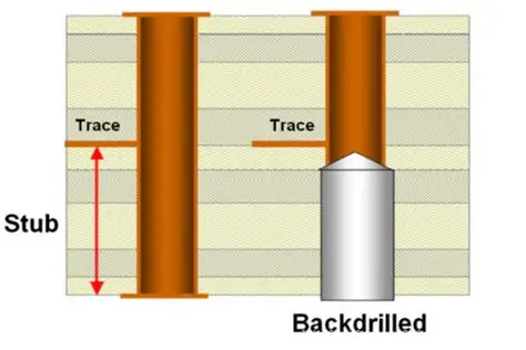
PCB back drilling involves drilling out the non-functional portion of a plated through-hole via from the opposite side of the board after plating. This technique targets the stub length beyond the last connected layer, reducing it to a minimal residue, typically under 20 mils, to improve signal propagation. In high-density interconnects, unchecked stubs cause impedance mismatches, leading to crosstalk, insertion loss, and eye diagram closure at gigabit speeds. For electrical engineers, back drilling ensures compliance with stringent signal integrity requirements in modern protocols.
The relevance stems from the shift toward faster data rates in PCBs, where via stubs act as quarter-wave resonators at frequencies above 1 GHz. Without back drilling, designers resort to blind or buried vias, which are costlier due to sequential lamination. Back drilling offers a middle ground, applicable to rigid boards with layer counts exceeding 12. It aligns with industry needs for scalable, high-performance interconnects while keeping PCB manufacturing costs manageable.
Factory insights reveal that back drilling enhances yield in assembly by minimizing drill breakout risks on inner layers. Properly executed, it supports denser routing and reduces the need for costly alternatives like via-in-pad. For budget-conscious projects, understanding its impact on overall back drilling price is crucial for procurement decisions.
Technical Principles of Backdrilling
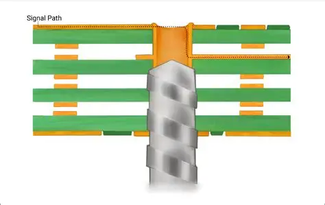
Back drilling uses a larger diameter drill bit, offset from the original via, to remove the stub while preserving the barrel plating on active layers. Depth control is paramount, achieved through optical sensing or mechanical stops to ensure accuracy within +/-0.002 inches. The process follows plating to avoid damaging the conductive path, and post-drill cleanup removes debris that could cause shorts. Engineers must specify stub length targets based on stackup and frequency requirements during design handover.
Material properties influence backdrill feasibility, as thicker cores demand higher aspect ratios and specialized tooling. Resin smear from aggressive drilling can degrade reliability, so controlled feed rates and peck drilling cycles are standard. Electrical testing post-backdrill verifies continuity and insulation resistance, confirming no opens or shorts. Adherence to IPC-6012E ensures the board meets qualification for rigid printed boards.
Signal integrity improves as backdrilled vias exhibit smoother impedance profiles, akin to microvias but at lower cost. Simulations using field solvers predict stub effects, guiding optimal depth. In practice, residue stubs below 10 mils suffice for many designs up to 10 Gbps, balancing performance with manufacturing tolerances.
Factors Affecting PCB Back Drilling Cost
Several variables drive PCB back drilling cost, starting with board thickness and layer count. Thicker stacks require deeper drills, increasing tool wear and setup time per panel. Via density amplifies expenses, as each backdrill cycle adds handling and alignment steps. Engineers should minimize backdrilled vias to essential signals only, prioritizing critical nets in high-speed zones.
Drill size and tolerance specifications further impact back drilling price. Larger clearances for stub removal ease processing but risk annular ring erosion, while tighter specs demand premium metrology. Material type plays a role; high-Tg laminates resist delamination better but may raise base PCB manufacturing costs. Panel utilization efficiency during production batches offsets per-unit expenses through economies of scale.
Tolerance on depth control is a major cost driver, with standard +/-0.003-inch windows suiting most designs versus tighter specs for exotic applications. Additional inspections, like X-ray or cross-sectioning, add to affordable back drilling challenges if not batched. Procurement teams benefit from quoting multiple suppliers on net counts and stackups to benchmark realistic budgets.
- Board Thickness: Higher thickness increases drill depth and tool life reduction
- Via Count: More vias mean extended machine time and setup
- Depth Tolerance: Tighter specs require advanced sensing equipment
- Panel Size/Yield: Larger panels improve cost per via through better utilization
Strategies for Affordable Backdrilling in Budget PCB Design
To achieve budget PCB design with back drilling, start by optimizing via placement during layout. Group backdrilled vias by depth to streamline tooling, reducing changeover times. Use symmetric stackups where possible to allow controlled depth drilling from both sides, halving stub lengths naturally. Simulations validate designs pre-tapeout, avoiding costly respins.
Material selection favors standard FR-4 grades over exotics unless thermal demands dictate otherwise, keeping base costs low. Specify realistic stub targets aligned with frequency needs, as over-specifying depth inflates back drilling price. Prototype with relaxed tolerances to iterate, then scale to production volumes for volume discounts.
Collaborate early with fabricators on design for manufacturability rules, such as minimum annular ring post-backdrill. Batch similar designs to share setup costs across runs. These approaches make affordable back drilling accessible without performance trade-offs.
Best Practices for Cost-Effective Backdrilling Implementation
Implement back drilling per J-STD-001 requirements for soldered assemblies, ensuring clean holes free of contaminants. Post-drill desmear processes like plasma or chemical etching enhance reliability, though they add minor costs justified by yield gains. Verify depths via automated optical inspection to catch outliers early.
In production, monitor tool offsets with pilot holes for registration. Factory-driven insights emphasize sequential backdrilling for multi-depth vias, processing shallower stubs first. Electrical engineers should include backdrill callouts in fab drawings, specifying depths per layer pair.
Regular calibration of depth sensors maintains consistency, preventing scrap. These practices, rooted in standard-aligned workflows, minimize PCB manufacturing costs while upholding quality.
Conclusion
Cost-effective PCB back drilling hinges on precise design, material choices, and manufacturing partnerships. By addressing key cost factors like via count and tolerances, engineers can integrate this technique into budget PCB design seamlessly. Affordable back drilling preserves signal integrity for high-speed applications without excessive expense. Prioritizing best practices ensures reliable outcomes, aligning performance with fiscal realities.
FAQs
Q1: What factors most influence PCB back drilling cost?
A1: Board thickness, via density, depth tolerances, and panel yield primarily drive PCB back drilling cost. Thicker boards demand deeper drills, increasing tool wear, while high via counts extend machine time. Standard tolerances keep back drilling price lower than precision specs. Optimizing layout reduces these impacts effectively.
Q2: How can I achieve affordable back drilling in budget PCB design?
A2: Group vias by depth, use symmetric stackups, and select standard materials for affordable back drilling. Simulate stub effects to specify only necessary depths, avoiding overdesign. Batch production leverages economies of scale on back drilling price. Early fabricator input refines manufacturability.
Q3: Does back drilling significantly raise overall PCB manufacturing costs?
A3: Back drilling adds 10-30% to via-related costs but remains lower than blind vias for many designs. It depends on volume and complexity; high-density boards see proportional increases. Balancing with essential use keeps total PCB manufacturing costs manageable. Factory efficiencies further mitigate impacts.
Q4: What standards guide reliable back drilling processes?
A4: IPC-6012E and J-STD-001 provide qualification criteria for backdrilled boards, covering plating integrity and depth control. These ensure performance in high-speed applications. Adhering to them minimizes rework and supports cost-effective implementation.
References
IPC-6012E — Qualification and Performance Specification for Rigid Printed Boards. IPC, 2017
J-STD-001H — Requirements for Soldered Electrical and Electronic Assemblies. IPC, 2018


