ALLPCB


Introduction
Double-layer printed circuit boards provide an essential balance between functionality and affordability for many electronic projects. Engineers often turn to these boards for prototypes, consumer devices, and industrial controls where complex multilayer stacks prove unnecessary. Achieving cost-effective PCB design requires careful attention to layout, materials, and manufacturing constraints from the outset. This approach not only reduces double layer PCB cost but also streamlines production without sacrificing reliability. By optimizing key elements, designers can minimize waste and fabrication expenses while meeting performance needs. The following sections outline structured strategies to enhance PCB design optimization.
Understanding Double-Layer PCBs and Their Cost Drivers
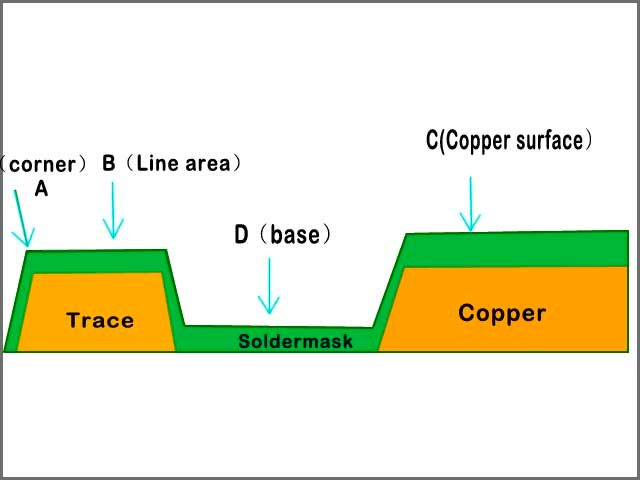
A double-layer PCB consists of a substrate with copper foil on both the top and bottom surfaces, interconnected via plated through-holes. This configuration supports moderate signal routing density, power distribution, and ground planes, making it suitable for applications like power supplies, sensors, and simple microcontrollers. Unlike single-layer boards, it allows signals to cross under traces on the opposite layer, reducing overall board size. However, costs arise from material usage, board dimensions, via count, and process complexity during fabrication.
Several factors directly influence double layer PCB cost. Larger board areas increase material consumption and panelization inefficiencies. High via density demands more drilling and plating steps, elevating labor and equipment time. Non-standard tolerances or shapes complicate tooling and setup, adding premiums. Copper thickness, finish types, and solder mask choices also contribute, with deviations from common specs driving up expenses. Understanding these drivers enables targeted PCB design optimization for low cost PCB production.
Core Technical Principles for Cost Reduction
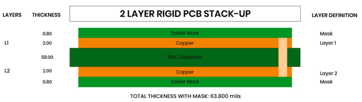
Effective cost-effective PCB design begins with material selection aligned to standard grades. FR-4 laminate with 1 oz copper weight serves most applications adequately, avoiding premiums for thicker foils or high-Tg variants unless thermal demands require them. Board thickness typically ranges from 0.8 mm to 1.6 mm, balancing rigidity and drill feasibility. Adhering to these norms minimizes raw material costs and ensures compatibility with standard fabrication flows.
Trace routing forms the backbone of double-layer efficiency. IPC-2221 provides guidelines for minimum trace widths and spacings based on current carrying capacity and voltage levels, preventing over-design that wastes copper. Engineers should calculate widths using these formulas to avoid unnecessary thickening, which increases etching time and material use. Spacing rules similarly prevent shorts while allowing dense layouts. Jumps between layers via through-holes must be planned to minimize count, as each via incurs drilling and plating costs.
Via optimization stands critical in double-layer boards. Standard through-hole vias suffice for interconnections, but excessive numbers inflate expenses through added process cycles. Designers limit vias by strategic component placement and orthogonal routing: horizontal traces on one layer, vertical on the other. This Manhattan-style approach reduces crossovers. Plated half-holes or edge castellations add cost, so reserve them for connectors only.
Practical Best Practices for Low Cost PCB Fabrication
Optimize board outline for rectangular shapes and standard panel fits. Irregular contours demand custom routing tools, raising setup fees. Aim for dimensions that tile efficiently on 18x24 inch panels, maximizing yield per panel. Group multiple boards via V-scoring or tabbing to share edge costs. This panelization technique directly lowers per-unit double layer PCB cost.
Component placement influences routing length and via needs profoundly. Position high-speed signals and power components first to centralize grounds and shorten paths. Cluster analog and digital sections to minimize crosstalk without split planes. Surface-mount devices predominate for density, but ensure pad sizes follow IPC standards for solderability. Avoid placements forcing long jumps or dense via fields, which complicate assembly.
Streamline silkscreen and solder mask layers for minimal ink usage. Use clear legends only where essential, opting for vector fonts to reduce file complexity. Solder mask over bare copper pours where possible, but define openings precisely for pads. These choices cut imaging and exposure steps. Electrical test points should integrate into existing pads rather than dedicated vias.
Advanced Optimization Techniques
Implement balanced copper pours on both layers to equalize plating stresses and prevent warpage. A ground pour on the bottom layer, with signal pour on top, aids EMI control without extras. Connect pours via multiple vias for low impedance returns. This practice enhances yield under IPC-6012 performance specs by reducing mechanical defects.
Thermal management in double-layer designs relies on copper areas rather than vias to inner planes. Widen traces under power components and add pours for heat spreading. Calculate junction temperatures conservatively, ensuring airflow or heatsinks handle dissipation. Avoid filled vias unless critical, as they demand microvia processes.
Design for manufacturability includes standard drill sizes like 0.3 mm to 0.6 mm for vias, avoiding micro-drills. Annular ring requirements per IPC-A-600 ensure reliability without excess copper. Fabricate prototypes at Class 2 quality to balance cost and function, escalating to Class 3 only for harsh environments.
Common Pitfalls and Troubleshooting Insights
Overlooking aspect ratios leads to drill breakage and yield loss. Keep via-to-board thickness below 10:1 for reliable plating. Dense routing near edges risks misalignment during lamination. Simulate impedance early if high-speed signals appear, adjusting widths per IPC-2221.
Excessive layer jumps create via farms, spiking costs. Review netlists for fanouts and consolidate grounds. Post-layout DRC checks catch spacing violations before Gerber output. Iterate with fabricator feedback on first runs to refine for volume.
Conclusion
Cost-effective PCB design for double-layer boards hinges on disciplined choices in layout, materials, and processes. By prioritizing standard specs, minimal vias, and efficient panelization, engineers achieve substantial savings in double layer PCB cost. PCB design optimization extends beyond schematics to fabrication awareness, yielding reliable, low cost PCBs. Apply these tips sequentially for prototypes scaling to production. Consistent adherence to guidelines like IPC standards ensures quality without excess expenditure.
FAQs
Q1: What is cost-effective PCB design for double-layer boards?
A1: Cost-effective PCB design focuses on minimizing material use, via count, and non-standard features while maintaining electrical performance. For double-layer boards, this involves standard FR-4, rectangular outlines, and orthogonal routing to reduce fabrication steps. Panelization further lowers per-unit double layer PCB cost. Engineers follow IPC-2221 for trace rules to avoid over-design. This approach suits most mid-complexity applications reliably.
Q2: How does board size affect low cost PCB production?
A2: Board size directly impacts material costs and panel efficiency in low cost PCB manufacturing. Smaller, rectangular boards fit more units per panel, reducing waste. Oversized or odd shapes incur custom tooling fees. Optimize dimensions to standard panel grids via V-scoring. Combine with minimal copper weight for further savings without performance loss. This PCB design optimization yields the lowest double layer PCB cost.
Q3: What role do vias play in double layer PCB cost?
A3: Vias significantly drive double layer PCB cost through drilling and plating operations. Minimize them by strategic routing and component grouping. Use standard sizes per IPC guidelines to avoid microvia premiums. Through-holes suffice for most interconnections in double-layer designs. Review layouts for unnecessary jumps to cut counts by 30–50 percent typically. Effective via management is core to cost-effective PCB design.
Q4: Why prioritize IPC standards in PCB design optimization?
A4: IPC standards like IPC-2221 ensure traces, spacings, and vias meet fabrication tolerances, preventing costly rework. They guide balanced designs for double-layer boards, optimizing for low cost PCB yields. Class 2 compliance balances economy and reliability. Deviations invite defects under IPC-6012 testing. Integrating these early streamlines the path from design to production.
References
IPC-2221B — Generic Standard on Printed Board Design. IPC, 2003
IPC-6012E — Qualification and Performance Specification for Rigid Printed Boards. IPC, 2017
IPC-A-600K — Acceptability of Printed Boards. IPC, 2020