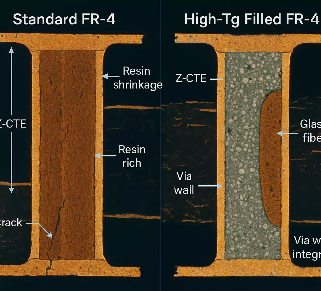
Designing a printed circuit board (PCB) that performs at its best requires careful attention to layer stackup and copper cladding. How can you optimize PCB performance through layer design? By strategically arranging signal layers, power planes, and ground planes, and using copper cladding effectively, you can enhance signal integrity, ensure impedance matching, and create a robust power distribution network. In this comprehensive guide, we’ll dive deep into the principles of PCB layer stackup, signal integrity analysis, impedance matching, power distribution network design, and copper plane placement techniques to help you achieve top-tier performance for your designs.
Why PCB Layer Stackup Matters for Performance
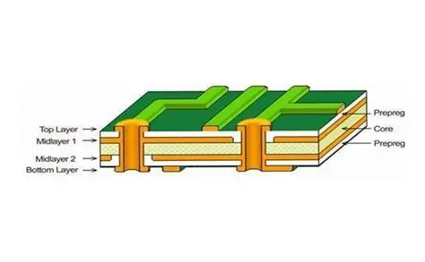
A PCB layer stackup is the arrangement of conductive and insulating layers in a multi-layer board. This structure directly impacts how signals travel, how power is distributed, and how much electromagnetic interference (EMI) your board produces or picks up. A poorly designed stackup can lead to issues like signal crosstalk, inconsistent impedance, or power delivery problems, which can degrade performance or cause failures in high-speed circuits.
For engineers working on complex designs—whether for consumer electronics, automotive systems, or industrial applications—optimizing the layer stackup is a critical step. A well-planned stackup ensures signal integrity by minimizing noise, maintains impedance for high-speed signals (often targeting 50 ohms for single-ended traces or 100 ohms for differential pairs), and supports efficient power delivery. Let’s explore the key elements of layer design and how they contribute to performance.
Understanding Signal Integrity Analysis in Layer Stackups
Signal integrity refers to the quality of an electrical signal as it travels through a PCB. Poor signal integrity can result in data errors, timing issues, or complete system failure, especially in high-speed designs operating at frequencies above 100 MHz. Signal integrity analysis focuses on reducing noise, crosstalk, and signal reflections, all of which are influenced by the PCB layer stackup.
One of the primary ways to ensure signal integrity is by placing signal layers adjacent to ground planes. This setup creates a controlled environment for signal traces, as the ground plane acts as a return path for current, reducing loop inductance and minimizing EMI. For example, in a 4-layer PCB, a common stackup might be:
- Top Layer: Signal
- Layer 2: Ground Plane
- Layer 3: Power Plane
- Bottom Layer: Signal
This configuration ensures that high-speed signals on the top and bottom layers have a nearby reference plane, which helps maintain signal quality. Additionally, spacing between layers (dielectric thickness) should be consistent to avoid impedance variations. A typical dielectric thickness might range from 0.1 mm to 0.2 mm for high-speed designs, depending on the material used, such as FR-4 with a dielectric constant of about 4.2.
Signal integrity can also be improved by routing critical traces away from noisy components and using shorter trace lengths to reduce signal delay. For instance, a signal delay of 1 ns per 15 cm of trace length is a rough guideline for FR-4 material, so minimizing trace length is crucial for timing-critical applications.
Impedance Matching: The Role of Layer Design
Impedance matching is essential for ensuring that signals transfer efficiently between components without reflections. Mismatched impedance can cause signal loss or distortion, especially in high-frequency applications like RF circuits or DDR memory interfaces. The PCB layer stackup plays a significant role in controlling impedance by determining the trace width, dielectric thickness, and proximity to reference planes.
For a standard 50-ohm single-ended trace, the trace width and dielectric height must be calculated based on the PCB material’s properties. As a general rule, for a 0.1 mm dielectric height using FR-4, a trace width of approximately 0.2 mm might achieve 50 ohms. However, these values vary based on the exact stackup and material, so using a field solver or impedance calculator during design is recommended. Many high-speed designs also use differential pairs, targeting 100 ohms, which requires precise spacing between the pair (often around 0.1 mm) and consistent dielectric properties.
To achieve controlled impedance, place signal layers close to a reference plane (ground or power) and maintain uniform dielectric thickness across the board. Avoid routing high-speed traces over splits in reference planes, as this can cause impedance discontinuities and signal reflections. A well-designed 6-layer stackup for impedance-controlled designs might look like this:
- Top Layer: Signal (high-speed)
- Layer 2: Ground Plane
- Layer 3: Signal (low-speed)
- Layer 4: Power Plane
- Layer 5: Ground Plane
- Bottom Layer: Signal (high-speed)
This arrangement ensures that high-speed signals have a nearby ground plane for consistent impedance while isolating power distribution to internal layers.
Power Distribution Network: Ensuring Stable Power Delivery
A power distribution network (PDN) is the system of planes, traces, and components that deliver power to all parts of a PCB. A poorly designed PDN can lead to voltage drops, noise, or insufficient current capacity, which can disrupt circuit operation. Layer stackup design is critical for creating an effective PDN, as it determines how power and ground planes are placed and how they interact with signal layers.
In most multi-layer PCBs, power and ground planes are placed on internal layers to provide low-impedance paths for current. Placing power and ground planes adjacent to each other creates a natural capacitance between them, which helps filter out high-frequency noise. For instance, in an 8-layer PCB, a common PDN configuration might be:
- Top Layer: Signal
- Layer 2: Ground Plane
- Layer 3: Power Plane (3.3V)
- Layer 4: Signal
- Layer 5: Signal
- Layer 6: Power Plane (5V)
- Layer 7: Ground Plane
- Bottom Layer: Signal
This setup minimizes the loop area for power delivery, reducing inductance and ensuring stable voltage levels. Decoupling capacitors, placed close to power pins of ICs, further enhance PDN performance by providing local energy storage. A typical value might be 0.1 μF for high-frequency decoupling, with larger capacitors (e.g., 10 μF) for bulk energy storage.
Another key aspect of PDN design is avoiding plane splits under critical components. A split in a power or ground plane can increase impedance and introduce noise, so ensure continuous planes wherever possible. If multiple voltage levels are required, dedicate separate planes or sections to each voltage to prevent interference.
Copper Plane Placement Techniques for Optimal Performance
Copper plane placement is a cornerstone of effective PCB design, influencing signal integrity, power delivery, and thermal management. Copper planes are typically used for ground and power distribution, but their placement within the layer stackup requires careful planning to avoid issues like crosstalk or excessive EMI.
One fundamental rule is to prioritize symmetry in the stackup. Symmetrical designs, where copper distribution is balanced across layers, prevent warping during manufacturing due to uneven thermal expansion. For example, in a 4-layer board, ensure that the top and bottom layers have similar copper coverage, and internal planes are evenly distributed.
Another technique is to use solid ground planes rather than gridded or hatched planes for high-speed designs. A solid plane provides a low-impedance return path for signals, reducing noise and EMI. If thermal relief is needed around through-hole components, use small cutouts rather than large gaps to maintain plane integrity.
Copper thickness also plays a role in performance. Standard copper thickness for outer layers is 1 oz/ft2 (approximately 35 μm), while inner layers might use 0.5 oz/ft2 (17 μm) for cost savings. However, for high-current applications, thicker copper (e.g., 2 oz/ft2 or 70 μm) on power planes can reduce resistance and improve heat dissipation.
Finally, consider copper pour on signal layers. Adding copper pour (connected to ground) on unused areas of signal layers can improve EMI shielding and provide additional return paths. However, ensure that these pours are properly stitched to the main ground plane with vias to avoid creating floating copper islands, which can act as antennas and increase noise.
Practical Tips for Designing an Optimized Layer Stackup
Now that we’ve covered the key concepts, let’s summarize some actionable tips for designing a PCB layer stackup that maximizes performance:
- Plan Early: Define the number of layers and their purpose (signal, power, ground) during the schematic phase to avoid redesigns later.
- Prioritize Ground Planes: Place ground planes near signal layers to provide return paths and reduce noise.
- Control Impedance: Use consistent dielectric thickness and calculate trace widths for target impedance values like 50 ohms or 100 ohms.
- Optimize PDN: Pair power and ground planes to create capacitance and use decoupling capacitors near ICs.
- Balance Copper: Ensure symmetrical copper distribution to prevent board warping and improve manufacturing reliability.
- Minimize Crosstalk: Separate high-speed signal layers with ground planes to reduce interference between traces.
By following these guidelines, you can create a layer stackup that supports high-speed signals, delivers stable power, and minimizes EMI, ultimately leading to a more reliable and efficient PCB design.
Conclusion: Building Better PCBs with Layer Design
Optimizing PCB performance through layer design is a blend of science and strategy. By carefully planning your PCB layer stackup, conducting signal integrity analysis, ensuring impedance matching, designing a robust power distribution network, and using effective copper plane placement techniques, you can create boards that meet the demands of modern electronics. Whether you’re working on a simple 4-layer board or a complex 10-layer design, these principles will help you achieve consistent, high-quality results.
At ALLPCB, we’re committed to supporting engineers with the tools and resources needed to bring their designs to life. A well-designed layer stackup is the foundation of any successful PCB, and with the right approach, you can tackle even the most challenging projects with confidence.
 ALLPCB


