ALLPCB


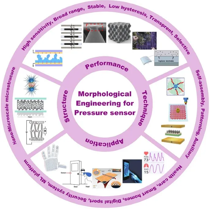
Overview
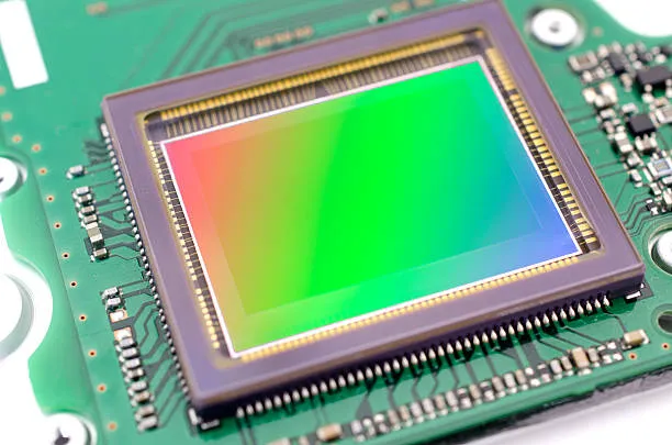
A charge-coupled device (CCD) sensor is a semiconductor device used for image capture. It records images by converting incident light into electrical charge and then converting those charges into digital signals for processing or storage. A CCD sensor consists of millions to tens of millions of tiny photosensitive elements, called pixels, arranged in a matrix. Each pixel independently senses the intensity and, in some designs, the color of incoming light and converts it into a proportional electrical charge.
Basic Principle
When light strikes the CCD, photons are absorbed by the photosensitive elements and generate charge proportional to the light intensity. Once a pixel has accumulated charge, the charge packets are transferred between adjacent potential wells inside the sensor via an internal charge-transfer mechanism. The transferred charge packets are then read out and converted into electrical signals, which can be digitized and processed to form an image.
MOS Capacitor as the Basic Unit
The basic building block of many CCD structures is the MOS capacitor, a simple metal-oxide-semiconductor device used to form potential wells that collect and store photo-generated charge.
Signal Generation, Storage, Transfer, and Detection
Signal generation: The first step in CCD operation is photoelectric conversion. Incident photons generate charge carriers in the semiconductor via the internal photoelectric effect.
Signal storage: The generated charges are collected and stored in potential wells, forming charge packets that represent the image signal.
Signal transfer (coupling): The stored charge packets are shifted from one pixel to the next until they reach the output stage. This sequential transfer is the "coupling" action that gives the device its name.
Signal detection: At the output stage, the transferred charges are converted into a current or voltage for readout and subsequent digitization.
Output types
- Current-output
- Floating-gate amplifier output
- Floating-diffusion amplifier output
CCD Structural Types
CCD sensors come in several structural variants, chosen according to application requirements:
- Interline Transfer CCD (IT-CCD): Uses interleaved photosensitive elements and vertical transfer channels. During exposure the photodiodes convert light to charge, which is then transferred line by line to the readout register.
- Frame Transfer CCD (FT-CCD): Has separate imaging and storage areas. After exposure, the image-area charges are quickly shifted to the storage area for readout, allowing rapid image capture with reduced smearing.
- Full Frame Transfer CCD (FFT-CCD): The entire image area is used for exposure; charges are shifted across the array into a storage register for readout, maximizing fill factor and sensitivity.
- Backside-Illuminated CCD (BSI-CCD): The photosensitive region is located on the back side of the substrate so light reaches the active area without passing through metal or polysilicon layers, improving quantum efficiency and low-light performance.
- Time Delay Integration CCD (TDI-CCD): Adds multiple storage stages that allow charges to be accumulated as the scene moves across the sensor, enabling high-sensitivity imaging of moving scenes.
Applications and Comparison with CMOS
CCD sensors are used in digital cameras, astronomical telescopes, medical imaging equipment, and scientific instruments where high sensitivity, low noise, and accurate color reproduction are important. Compared with CMOS sensors, CCDs traditionally offer higher image quality and lower noise in some applications, though CMOS technology has advanced and offers advantages in integration and cost in many use cases.