ALLPCB


Introduction
Companies that develop medical diagnostic devices must deliver accurate and cost-effective products while reducing device size. Shrinking form factors and improving measurement precision are critical to lowering care costs and improving patient outcomes, especially as populations age.
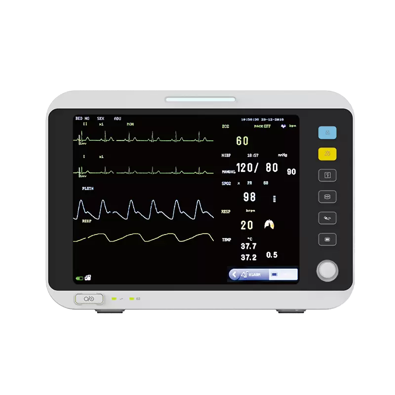
Advances in monitoring and remote care provide better diagnostic tools for home patients, emergency responders, and hospitals. Devices such as blood pressure monitors, glucose meters, and defibrillators require clean analog signals for accurate measurement; otherwise patient safety can be compromised. A well-designed analog signal path reduces susceptibility to external noise, extends dynamic range, and improves accuracy. Component selection must also meet the final product's performance requirements.
High-performance Needs in Small Packages
Historically, clinical equipment was considered more precise than portable consumer devices. New trends are changing that view: portable devices now serve not only general consumers but also tech-literate patients, so user expectations go beyond simple temperature, ECG, or blood pressure measurements. They expect broader monitoring and measurement capabilities.
To meet rising demand for home diagnostic instruments, suppliers are using advanced inventory management and design innovations to add more functionality. A critical factor in bringing home medical devices to market is development time: shorter time-to-market allows products to reach users sooner. Reducing development cycles depends on system designers producing flexible, cost-effective designs.
Process Technology Influences System Design
Electrical specifications guide component selection, but the semiconductor process used to manufacture integrated circuits also matters. For example, a typical glucose meter often requires an operational amplifier with extremely low input bias current, so designers may choose a JFET-input amplifier. However, temperature behavior must be considered.
JFETs can have very low initial input bias currents but are sensitive to temperature: the input bias current roughly doubles for every 10°C increase. This drift can be estimated with the formula:
Ib(T) = Ib(T0) x 2^((T - T0)/10)
For example, a JFET-input op amp such as National Semiconductor's LF411 has an input bias current of 50 pA at 25°C. A better option in some designs is the LMP7731, a bipolar-input op amp with an input bias current of 1.5 nA. Using the formula above, at 85°C the LF411's input bias current rises to about 3.2 nA, more than twice the LMP7731's bias current.
Evaluating Trade-offs
Speed, noise, and power consumption are often competing priorities. A low-noise device typically consumes more current, while a low-power device may offer limited bandwidth. One approach for certain applications is to use a decompensated amplifier. Compared with unity-gain-stable, high-speed amplifiers, decompensated amplifiers can offer larger bandwidth for a given power consumption and lower cost.
Decompensated amplifiers are well suited for transimpedance (current-to-voltage) circuits. A common application in medical instruments is measuring peripheral oxygen saturation (SpO2).
Using Shortcuts to Shorten Design Time
Noise is one of the most important parameters in medical instruments because it can cause significant interference in the circuit itself and nearby equipment. Calculating the total noise contribution from the power supply, amplifiers, data converters, and external components is tedious but necessary to estimate the signal-to-noise ratio.
Medical circuits often operate at low frequencies, so designers typically focus on noise in the 0.1 to 10 Hz band, commonly expressed as peak-to-peak noise. Some datasheets do not provide time-domain peak-to-peak values and only include voltage or current noise density plots. Besides requesting measurements from component vendors, a quick method exists to estimate peak-to-peak noise.
Suppose you want to estimate the 0.1 to 10 Hz peak-to-peak voltage noise for the LMP7731. First, pick a point in the specified band, for example 1 Hz, where the noise density is 5.1 nV/√Hz (see Figure 2). Compute the RMS noise over the band using:
en_rms = enf * sqrt(ln(10 / 0.1))
where enf is the noise density at 1 Hz. Using the values above yields an en_rms of about 10.9 nV. To convert RMS to peak-to-peak, multiply by 6.6, giving approximately 72.2 nV. This estimate is close to the datasheet specification of 78 nV.
If the datasheet's noise density plot does not include a 1 Hz value, use this relation to estimate the noise at a given frequency:
en(f) = enb * sqrt(fce / f)
where enb is the broadband noise (typically specified at 1 kHz), fce is the 1/f corner frequency, and f is the frequency of interest (1 Hz in the example above).