 ALLPCB


High-density printed circuit boards place components closer together and route signals through smaller features than earlier generations allowed. Solder mask, the protective polymer layer applied over copper traces, must perform reliably under these constraints to prevent shorts, control solder flow, and protect against environmental stress. Engineers working on boards for telecommunications, computing, and automotive systems increasingly rely on specialized solder mask methods to maintain yield and long-term performance. These techniques address the unique challenges of fine-pitch components and ball-grid array packages while remaining compatible with standard fabrication processes.
Why Advanced Solder Mask Techniques Matter
In high-density layouts, the distance between copper features shrinks, raising the risk of solder bridging during reflow. Traditional blanket solder mask coverage no longer suffices when vias sit directly under component pads or when trace widths fall below 100 micrometers. Techniques such as solder mask via tenting, solder mask via plugging, and solder mask dams provide targeted coverage that improves insulation and reduces the chance of contaminants reaching exposed copper. Solder mask defined pads and non-solder mask defined pads further influence how solder wets to the pad, affecting joint shape and reliability for fine-pitch components and BGA solder mask applications. Without these refinements, assembly defects rise and boards may fail environmental qualification tests.
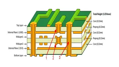
Technical Principles of Solder Mask Application
Solder mask via tenting covers the via opening with a thin layer of mask material, sealing it from both sides or one side depending on board thickness and process capability. This approach prevents solder from wicking into the via during reflow while still allowing the via to function electrically. Solder mask via plugging fills the via barrel completely with mask or a compatible filler before the final mask coat, offering stronger mechanical protection and better planarity for subsequent assembly steps. Solder mask dams create narrow barriers of mask between adjacent pads or traces, limiting solder spread and helping maintain clearance in dense areas.
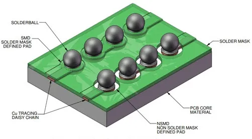
Solder mask defined pads use the mask opening to determine the final copper land size exposed for soldering, which can improve registration accuracy but requires tight control of mask alignment. Non-solder mask defined pads expose a larger copper area than the mask opening, allowing the copper pad itself to define the land and providing more tolerance for mask misregistration. Both approaches appear in BGA solder mask designs, where the choice affects solder joint volume and stress distribution during thermal cycling. Industry standards such as IPC-6012E outline qualification requirements that these mask features must meet for rigid boards.
Best Practices for High-Density Designs
Designers begin by reviewing the stack-up and component footprint to decide which vias require tenting versus plugging. Vias under BGAs often receive plugging to maintain a flat surface for paste printing, while vias in less critical areas may use tenting to reduce process steps. When placing solder mask dams, the minimum dam width follows fabricator capabilities, typically 50 to 75 micrometers, to avoid mask lifting or incomplete coverage. For fine-pitch components, maintaining consistent mask thickness across the board helps prevent warpage-related defects during reflow.
Engineers also evaluate whether solder mask defined or non-solder mask defined pads better suit the thermal and mechanical requirements of each package. Non-solder mask defined pads generally offer better copper adhesion and larger effective pad area, which can improve current-carrying capacity. Solder mask defined pads provide tighter control over solder volume, which benefits very fine pitches where excess solder increases bridging risk. Collaboration with the fabrication team early in the layout phase confirms that the chosen mask openings and via treatments align with the available equipment and materials.
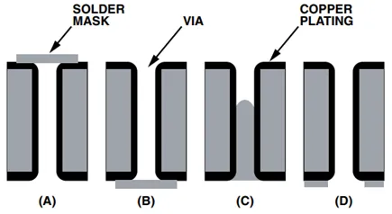
Considerations for Fine-Pitch Components and BGA Packages
Fine-pitch components demand precise mask registration because even small offsets can expose unintended copper or cover part of a pad. BGA solder mask designs often combine plugged vias under the package with carefully sized mask openings around each ball to control paste volume and prevent voiding. Thermal expansion differences between the board and package can stress the solder joints, so mask thickness and adhesion properties receive attention during material selection. IPC-A-600K provides visual acceptance criteria that help inspectors verify mask coverage, dam integrity, and via treatment quality on finished boards.
When multiple fine-pitch devices sit close together, solder mask dams between them reduce the chance of solder migration across the narrow gaps. Designers also consider mask color and finish, as matte finishes can improve automated optical inspection contrast while glossy finishes may aid visual inspection. Process parameters such as mask cure temperature and exposure energy affect final hardness and chemical resistance, influencing long-term reliability under humidity and temperature cycling.
Conclusion
Advanced solder mask techniques give engineers practical tools to manage the electrical and mechanical demands of high-density PCBs. Proper application of via tenting, via plugging, dams, and pad definitions supports higher component density without sacrificing assembly yield or long-term reliability. Early coordination between design and fabrication teams, combined with adherence to established qualification and acceptance standards, helps ensure consistent results across production runs.
FAQs
Q1: What is solder mask via tenting and when is it preferred?
A1: Solder mask via tenting applies a thin mask layer over via openings to seal them from solder during reflow. It is often chosen for vias not located under components where complete filling is unnecessary and process simplification is desirable. The method maintains electrical performance while reducing the risk of solder wicking.
Q2: How does solder mask via plugging differ from tenting in high-density boards?
A2: Solder mask via plugging fills the via barrel completely, providing greater mechanical strength and surface planarity. This approach suits vias beneath BGAs or other area-array packages where flatness aids paste deposition and joint formation. Tenting leaves the barrel open or partially covered and is used where full filling adds unnecessary cost.
Q3: What are the differences between solder mask defined pads and non-solder mask defined pads?
A3: Solder mask defined pads rely on the mask opening to set the exposed copper area, offering tighter control over solder volume. Non-solder mask defined pads expose more copper than the mask opening, providing greater tolerance to mask misalignment and improved copper adhesion. The choice depends on pitch, current requirements, and thermal cycling expectations.
Q4: Why are solder mask dams important for fine-pitch components?
A4: Solder mask dams create physical barriers that limit solder flow between closely spaced pads or traces. In fine-pitch layouts, they help prevent bridging and maintain required electrical clearances. Proper dam width and height are verified against fabricator capabilities and acceptance criteria in relevant industry standards.
References
IPC-6012E — Qualification and Performance Specification for Rigid Printed Boards. IPC, 2017
IPC-A-600K — Acceptability of Printed Boards. IPC, 2020
JEDEC J-STD-020E — Moisture/Reflow Sensitivity Classification. JEDEC, 2014





