If you're looking to understand the PCB inner layer lamination process, vacuum lamination, and how to achieve superior bonding strength, you've come to the right place. At ALLPCB, we know that robust bonding in multilayer printed circuit boards (PCBs) is critical for performance, durability, and reliability. In this comprehensive guide, we'll dive into advanced lamination techniques, breaking down the processes, materials, and best practices to ensure your PCBs meet the highest standards.
What is PCB Inner Layer Lamination and Why Does It Matter?
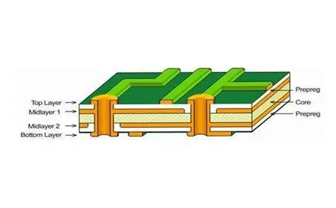
The PCB inner layer lamination process is a key step in manufacturing multilayer boards. It involves bonding multiple layers of conductive copper foil and insulating dielectric materials together under heat and pressure to form a single, unified structure. This process ensures that the inner circuitry connects seamlessly with outer layers, enabling complex designs and high-density interconnections.
Why is this important? Poor lamination can lead to delamination, weak bonding strength, and signal integrity issues, which can cause failures in electronic devices. For engineers and manufacturers, mastering lamination techniques directly impacts the quality and reliability of the final product. Whether you're working on high-speed digital circuits or power electronics, robust bonding is non-negotiable.
Core Principles of the PCB Inner Layer Lamination Process
Before diving into advanced techniques, let's break down the fundamental steps of the PCB inner layer lamination process. This will help you understand the foundation on which modern methods are built.
- Material Preparation: The process starts with preparing the inner layers, prepregs (partially cured resin sheets), and copper foils. These materials must be clean and free of contaminants to ensure strong bonding.
- Layer Stacking: Layers are carefully aligned and stacked. Precise registration is critical to avoid misalignment, which can disrupt circuitry connections.
- Heat and Pressure Application: The stack is placed in a lamination press, where heat (typically 170-200°C) and pressure (around 200-400 psi) are applied to cure the resin in the prepreg, bonding the layers together.
- Cooling: After lamination, the board is cooled under controlled conditions to prevent thermal stress and warping.
These steps are the backbone of lamination, but achieving optimal bonding strength requires advanced techniques and attention to detail. Issues like air entrapment, uneven pressure, or improper curing can weaken bonds and compromise board integrity.
Advanced Techniques in PCB Inner Layer Lamination
Modern PCB manufacturing has evolved to address challenges in traditional lamination, introducing advanced methods to enhance bonding strength and reliability. Below are some cutting-edge techniques that are shaping the industry.
1. Vacuum Lamination for Superior Bonding
Vacuum lamination is a game-changer in achieving robust bonding for multilayer PCBs. Unlike conventional lamination, which relies solely on heat and pressure, vacuum lamination removes air from the lamination chamber before pressing. This eliminates air bubbles and voids between layers, which are common causes of delamination and reduced bonding strength.
In a typical vacuum lamination setup, the pressure in the chamber is reduced to below 10 Torr, ensuring that trapped air is minimized. The result is a denser, more uniform bond. Studies have shown that vacuum-laminated boards can achieve up to 30% higher bonding strength compared to non-vacuum methods, making this technique ideal for high-reliability applications like aerospace and medical electronics.
2. Sequential Lamination for High-Density Interconnects (HDI)
For complex designs like HDI boards, sequential lamination is often used. This technique involves laminating subsets of layers in multiple cycles rather than bonding all layers at once. By building the board in stages, manufacturers can incorporate microvias and fine-pitch components with greater precision.
Sequential lamination enhances bonding strength by reducing stress on individual layers during the process. It also allows for better control over dielectric thickness, which is crucial for maintaining impedance values (often targeted at 50 ohms for high-speed signals). This method is particularly useful for boards with 8 or more layers, where uniform bonding becomes increasingly challenging.
3. Optimized Prepreg Selection for Enhanced Bonding Strength
The choice of prepreg material plays a significant role in bonding strength. Prepregs with higher resin content (around 60-70%) provide better flow during lamination, filling gaps and ensuring a stronger bond. Additionally, low-loss prepregs with dielectric constants (Dk) of 3.5-4.0 are often used in high-frequency applications to minimize signal loss while maintaining robust adhesion.
Manufacturers can also select prepregs with specific glass transition temperatures (Tg), typically above 170°C, to withstand thermal stresses during operation. Matching the prepreg's properties to the board's requirements is a critical step in achieving long-term reliability.
Factors Affecting Bonding Strength in PCB Lamination
Even with advanced techniques, several factors can influence the bonding strength of a PCB. Understanding and controlling these variables is essential for consistent results.
- Temperature Control: Excessive heat can degrade resin, while insufficient heat may prevent full curing. Maintaining a tight temperature range (e.g., ±5°C of the target 180°C) is crucial.
- Pressure Uniformity: Uneven pressure can cause weak spots in the bond. Modern presses use hydraulic systems to ensure uniform force distribution, often within ±10 psi across the board surface.
- Material Cleanliness: Contaminants like dust or oil on copper surfaces can weaken adhesion. Pre-lamination cleaning processes, such as plasma etching, can improve surface readiness.
- Vacuum Levels: In vacuum lamination, achieving and maintaining low pressure (below 10 Torr) is vital to eliminate air entrapment, which can reduce bonding strength by up to 20% if not addressed.
By closely monitoring these factors, manufacturers can minimize defects and ensure that bonding strength meets or exceeds industry standards, such as those set by IPC (Institute of Printed Circuits).
Benefits of Strong Bonding in Multilayer PCBs
Investing in advanced lamination techniques and robust bonding offers several advantages for PCB performance and longevity.
- Improved Reliability: Strong bonds prevent delamination, even under harsh conditions like thermal cycling or mechanical stress. This is critical for applications where failure is not an option, such as in automotive safety systems.
- Better Signal Integrity: Uniform bonding reduces impedance mismatches, ensuring consistent signal speeds (often exceeding 5 Gbps in high-speed designs) and minimizing crosstalk.
- Enhanced Durability: Boards with high bonding strength can withstand environmental factors like humidity and vibration, extending the lifespan of electronic devices.
Best Practices for Achieving Optimal Bonding Strength
To help engineers and manufacturers achieve the best results in the PCB inner layer lamination process, here are some actionable best practices:
- Use Vacuum Lamination for Critical Applications: If your design requires high reliability, opt for vacuum lamination to eliminate voids and enhance bonding strength.
- Select Materials Carefully: Match prepreg and core materials to your board's thermal and electrical requirements. For high-frequency designs, prioritize low-loss materials with stable Dk values.
- Maintain Process Control: Monitor temperature, pressure, and vacuum levels closely during lamination to avoid deviations that could weaken bonds.
- Conduct Post-Lamination Testing: Use techniques like cross-sectional analysis or peel strength testing (targeting values above 6 N/cm) to verify bonding quality before moving to assembly.
Following these practices can significantly improve the outcome of your lamination process, ensuring that your PCBs perform reliably in their intended applications.
Common Challenges in PCB Lamination and How to Overcome Them
Even with advanced techniques, challenges can arise during lamination. Here's how to address some common issues:
- Delamination: Often caused by air entrapment or poor material compatibility. Using vacuum lamination and ensuring proper material selection can mitigate this risk.
- Warping: Uneven cooling or excessive thermal stress can distort the board. Implement controlled cooling cycles (e.g., reducing temperature by 2°C per minute) to prevent this.
- Resin Starvation: Insufficient resin flow can lead to weak bonds. Choose prepregs with adequate resin content and optimize lamination parameters like pressure and time.
By proactively addressing these challenges, manufacturers can maintain high bonding strength and produce defect-free boards.
The Future of PCB Lamination Techniques
As electronics continue to shrink and performance demands increase, the future of PCB lamination is geared toward even greater precision and efficiency. Emerging technologies like laser-assisted lamination and advanced resin formulations are being explored to further enhance bonding strength and reduce process times. Additionally, automation and real-time monitoring systems are making lamination more consistent, with defect rates dropping below 1% in some high-end facilities.
For engineers, staying updated on these advancements is key to designing and manufacturing cutting-edge PCBs that meet tomorrow's challenges.
Conclusion: Building Stronger PCBs with Advanced Lamination
The PCB inner layer lamination process is at the heart of multilayer board manufacturing, and mastering it is essential for ensuring robust bonding strength. Techniques like vacuum lamination and sequential lamination, combined with careful material selection and process control, can significantly enhance the quality and reliability of your PCBs.
At ALLPCB, we're committed to helping you navigate the complexities of PCB manufacturing with state-of-the-art solutions and expert guidance. By adopting the advanced techniques and best practices outlined in this guide, you can achieve stronger bonds, better performance, and longer-lasting boards for your electronic projects.
 ALLPCB


