 ALLPCB


Introduction
Selective PCB plating represents a targeted approach in printed circuit board manufacturing where metal deposition occurs only on designated areas rather than the entire board surface. This technique addresses the need for enhanced conductivity, corrosion resistance, and durability in specific regions like edge connectors or contact pads while minimizing material waste. Manufacturers increasingly adopt selective PCB plating methods to meet performance demands in high-reliability electronics without incurring the expenses of full-panel plating. By focusing on precision, this process aligns with factory workflows that prioritize efficiency and compliance with industry benchmarks. As electric engineers specify designs for demanding applications, understanding selective plating becomes essential for optimizing production outcomes.
What Is Selective PCB Plating and Why It Matters
Selective PCB plating involves applying metallic finishes, such as gold or nickel, to precise locations on the board using protective barriers or extensions that limit deposition. Unlike blanket plating, which covers the whole panel, selective methods ensure that costly materials deposit only where functional requirements dictate, such as high-wear contacts or signal interfaces. This matters in manufacturing because it directly impacts reliability in environments exposed to friction, oxidation, or repeated insertions, common in connectors and modules. Factory-driven processes benefit from reduced chemical usage and simpler post-plating cleanup, enhancing throughput in volume production. For electric engineers, selective plating maintains signal integrity and solderability per IPC-6012 qualification specifications for rigid printed boards, ensuring boards meet performance criteria without excess costs.
The relevance extends to modern electronics where miniaturization and high-density layouts demand localized enhancements. Selective plating prevents issues like migration or delamination in unneeded areas, preserving overall board integrity. Manufacturers gain a competitive edge by integrating these methods into standard electroless or electrolytic lines, adapting to diverse customer specs efficiently.
Selective PCB Plating Methods
Selective PCB plating methods primarily include mask plating and tab plating, each suited to different production scales and design geometries. These techniques leverage resists, masks, or temporary extensions to confine plating chemistry to target zones, ensuring uniform thickness and adhesion. Factories select methods based on board complexity, volume, and finish type, such as electroless nickel immersion gold (ENIG) or hard gold. Both approaches integrate seamlessly into the plating sequence after pattern imaging and before final finishing, maintaining process flow.
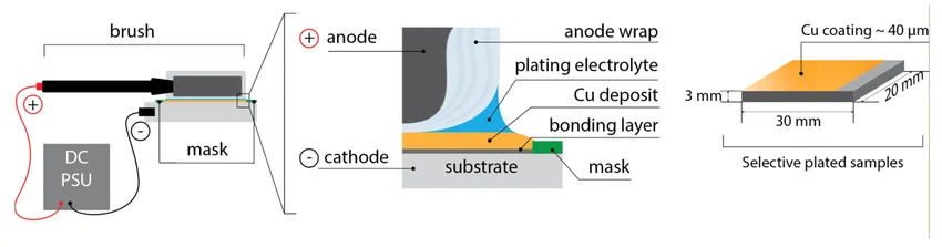
Mask Plating
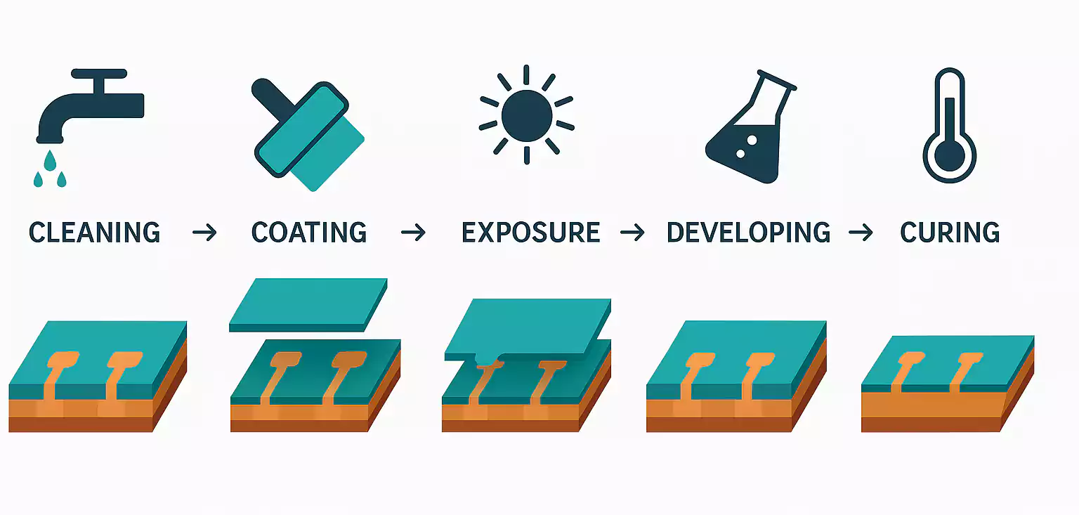
Mask plating employs a temporary resist or dry film to shield non-plating areas during immersion or electrolytic deposition. The process begins with precise application of the mask via screen printing or lamination, followed by exposure and development to expose only the desired pads or traces. After plating, the mask strips away cleanly, leaving sharp boundaries without undercutting. This method excels in high-volume runs where automation handles mask alignment, reducing handling time in the plating tank.
Advantages include minimal material waste since chemistry contacts only exposed surfaces, and it supports fine-pitch features down to standard tolerances. However, mask adhesion must withstand bath agitation to avoid defects like bridging. Electric engineers appreciate mask plating for its compatibility with surface finishes like selective ENIG, where nickel underlayers prevent gold diffusion.
Tab Plating
Tab plating, often called finger or edge tab plating, involves extending copper tabs from the board edge during initial lamination, then plating these protrusions before milling them flush to form contacts. Panels route with oversized tabs connected via breakaway rails, allowing rack plating without masking the main board. Post-plating, tabs shear and bevel to final dimensions, integrating seamlessly into the board profile. This method suits gold finger applications requiring thick, hard gold layers for durability.
Tab plating offers uniform thickness across multiple fingers due to direct rack contact, ideal for consistent wear resistance. Factories favor it for prototype or low-volume jobs where masking setup proves costly. Drawbacks include added panel real estate and milling waste, though modern CNC routing minimizes this.
Selective Plating Cost Savings
Selective plating delivers significant cost savings by limiting precious metals like gold to functional areas, avoiding the expense of full-panel coverage. In mask plating, resists prevent unnecessary deposition, directly reducing chemical consumption and rinse water volume in plating lines. Tab plating achieves similar economies by concentrating plating on extensions, with milling removing only excess carrier material rather than wasting finish across the board. Manufacturers report streamlined wastewater treatment and shorter cycle times, as selective racks process fewer panels per bath refresh.
Beyond materials, selective methods cut post-processing labor since no broad stripping or etching occurs. For high-reliability Class 3 boards, these savings compound in production scaling, aligning with IPC-A-600 acceptability criteria that emphasize defect-free finishes without over-plating. Electric engineers designing for cost-sensitive applications find selective plating balances performance and budget, especially in edge connector modules.
Selective Plating Applications
Selective plating applications span connectors, memory modules, and automotive electronics where localized durability proves critical. Gold fingers on RAM or SSD cards rely on tab plating for repeated insertions, ensuring low contact resistance over cycles. Mask plating suits selective ENIG on high-frequency RF pads, preventing solder mask interactions while maintaining flatness for assembly. In power modules, edge plating via selective methods enhances current handling and EMI shielding without compromising inner layer integrity.
These applications thrive in environments demanding corrosion resistance, such as aerospace interfaces or telecom backplanes. Factories apply selective plating to half-holes or castellations in embedded modules, meeting mechanical stress without full exposure. Engineers specify it for mixed-signal boards, isolating plated contacts from sensitive analog areas.
Best Practices for Selective PCB Plating
Implement robust surface preparation before selective plating to ensure adhesion, including micro-etch and activation for oxide-free copper. Maintain bath chemistry within manufacturer specs, monitoring pH, temperature, and additive levels to achieve uniform deposition. For mask plating, verify resist tenting over fine features to prevent bleed, using laser direct imaging for precision. In tab plating, design break lines with adequate copper weight to withstand rack stresses during electrolytic gold strike.
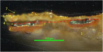
Conduct in-line thickness gauging and cross-section analysis per IPC-6012 performance specs to validate layer integrity. Avoid over-plating by timing baths precisely, and integrate peelable masks for complex geometries. Post-plating, inspect for voids or porosity via dye penetrant, addressing issues early to minimize scrap.
Train operators on handling to prevent mask scratches, and segregate selective panels from full-plating lines to avoid contamination. Collaborate with design teams on panelization, optimizing tab spacing for rack efficiency.
Conclusion
Selective PCB plating methods like mask and tab plating empower manufacturers to deliver high-performance boards with targeted enhancements and notable cost savings. By confining finishes to critical areas, these techniques uphold reliability in demanding applications while streamlining factory operations. Electric engineers benefit from precise control over conductivity and durability, guided by standards like IPC-6012 and IPC-A-600. Adopting best practices ensures consistent quality, reducing defects and accelerating time-to-market. Ultimately, selective plating stands as a cornerstone for efficient, standard-compliant PCB production.
FAQs
Q1: What are the main selective PCB plating methods?
A1: Mask plating and tab plating dominate selective PCB plating methods. Mask plating uses resists to expose only target areas for deposition, ideal for fine-pitch ENIG. Tab plating extends fingers for rack plating before milling, suiting thick gold contacts. Both minimize waste and integrate into standard lines, per IPC guidelines for uniform thickness. Factories choose based on volume and geometry for optimal results.
Q2: How does selective plating achieve cost savings?
A2: Selective plating cost savings stem from reduced precious metal usage, as chemistry applies only to designated zones via masks or tabs. This cuts material, chemical, and treatment expenses compared to full panels. Shorter cycles and less rework further lower overhead. Manufacturers realize these benefits in high-volume connector production, maintaining IPC-A-600 compliance without excess spending.
Q3: What are common selective plating applications?
A3: Selective plating applications include gold fingers for memory cards, edge connectors in backplanes, and RF contact pads. Tab plating excels in wear-prone interfaces, while mask plating fits mixed finishes on dense boards. These enhance conductivity and corrosion resistance in telecom and automotive uses. Engineers specify them for reliability under IPC-6012 performance criteria.
Q4: When should manufacturers choose mask plating over tab plating?
A4: Opt for mask plating in high-volume, fine-pitch designs where automation handles resists efficiently, avoiding panel extensions. Tab plating suits prototypes or thick gold fingers needing uniform rack deposition. Consider geometry, cost, and milling tolerance; mask offers sharper edges but requires precise stripping. Both align with factory best practices for selective plating applications.
References
IPC-6012E — Qualification and Performance Specification for Rigid Printed Boards. IPC, 2017
IPC-A-600K — Acceptability of Printed Boards. IPC, 2020
IPC-2221B — Generic Standard on Printed Board Design. IPC, 2012


