ALLPCB


Introduction
Renewable energy systems such as solar inverters and wind turbines demand printed circuit boards that handle substantial electrical loads while maintaining long-term reliability under variable environmental conditions. Four-ounce copper PCBs provide thicker conductive layers that support higher current densities compared with standard one-ounce or two-ounce constructions. This thickness reduces resistive losses and improves thermal dissipation in power conversion circuits. Engineers designing equipment for solar installations and wind farms increasingly specify these boards to meet performance targets without excessive board area. The approach aligns with requirements for robust power electronics that operate continuously in remote or exposed locations.
What Is a 4 oz Copper PCB and Why It Matters
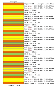
A four-ounce copper PCB features copper foil weighing four ounces per square foot, resulting in an approximate thickness of 140 micrometers per layer. This construction delivers greater cross-sectional area for current flow than thinner foils, directly lowering voltage drop in high-power traces. In renewable energy contexts, the added copper mass also enhances heat spreading, which helps maintain component temperatures within acceptable limits during peak generation periods. Industry professionals recognize that such boards contribute to overall system efficiency by minimizing energy wasted as heat. Procurement teams and design engineers evaluate these characteristics when specifying boards for solar inverter power stages or wind turbine converter modules. The choice supports compact layouts that still satisfy demanding electrical and thermal specifications.
Technical Principles of Thick Copper in Power Applications
Current-carrying capacity scales with copper thickness because resistance is inversely proportional to conductor cross-section. In a four-ounce layer, wider traces can carry tens of amperes while keeping temperature rise modest, which is essential for continuous operation in solar inverters. Thermal conductivity improves as well, allowing heat generated by switching devices to spread laterally before reaching the heatsink interface. Mechanical robustness increases because the thicker foil resists cracking during thermal cycling or vibration exposure typical of wind turbine nacelles. These mechanisms operate together to extend operational life and reduce maintenance intervals in renewable installations. Design rules must account for etch factors and plating uniformity to realize the full benefit of the added copper.
Practical Design and Manufacturing Considerations
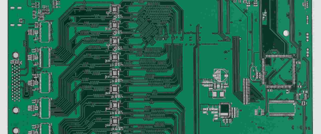
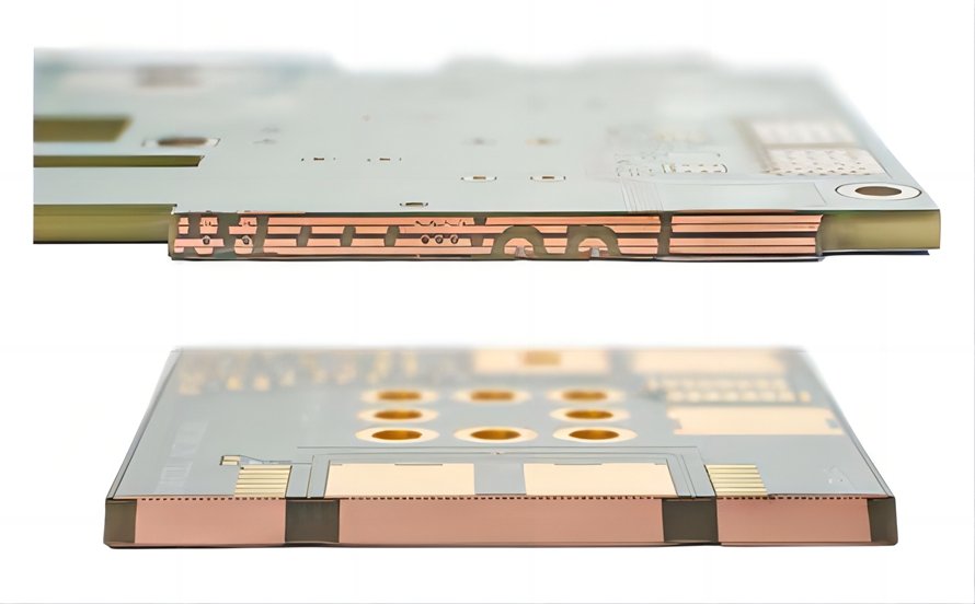
Engineers begin by calculating required trace widths using established current-carrying charts that incorporate copper weight, allowable temperature rise, and ambient conditions. For solar inverter boards, power paths from DC input to AC output stages often use four-ounce copper on outer layers while inner signal layers remain thinner. Wind turbine designs incorporate the same approach for generator-side converters and grid interface circuits. Manufacturing follows qualification procedures outlined in IPC-6012E to confirm that plated through-holes and surface finishes meet performance criteria for rigid boards. Controlled impedance routing and proper via placement further ensure signal integrity alongside the high-current paths. Assembly processes must accommodate the increased thermal mass during reflow without introducing defects such as tombstoning or insufficient solder fillets.
Best Practices for Reliability in Renewable Energy Environments
Reliability testing emphasizes thermal shock, humidity exposure, and mechanical vibration to simulate field conditions encountered by solar and wind equipment. Four-ounce copper boards demonstrate improved resistance to electromigration and thermal fatigue when fabricated according to IPC-A-600K acceptability criteria. Conformal coating or encapsulation adds another layer of protection against moisture and salt spray in coastal wind installations. Designers also specify appropriate laminate materials with high glass-transition temperatures to maintain dimensional stability across wide temperature swings. Regular inspection of solder joints and copper integrity during production helps identify process variations before boards reach the field. These steps collectively reduce the likelihood of premature failure and support extended warranty periods offered by renewable energy system integrators.
Troubleshooting Common Issues in Thick Copper Designs
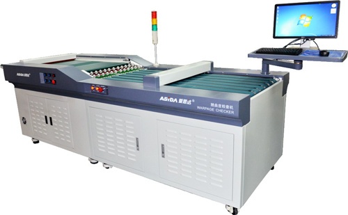
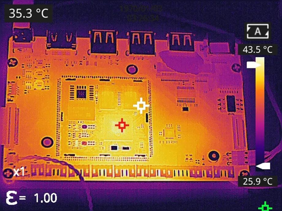
Uneven etching can leave residual copper that creates unintended shorts or alters impedance in mixed-signal sections of an inverter board. Insufficient via fill or plating thickness may cause localized heating under high current, which is detectable through infrared imaging during prototype validation. Warpage arising from asymmetric copper distribution requires balanced stackups and controlled lamination cycles to keep boards within flatness tolerances for automated assembly. In wind turbine applications, vibration-induced fatigue at copper-to-laminate interfaces can be mitigated by optimizing pad sizes and using appropriate surface finishes. Systematic root-cause analysis during pilot production prevents these issues from affecting volume manufacturing.
Conclusion
Four-ounce copper PCBs deliver measurable improvements in current handling, thermal performance, and mechanical durability for renewable energy power electronics. Their adoption in solar inverter and wind turbine designs supports higher efficiency targets and longer service intervals without enlarging board dimensions. Careful attention to layout, material selection, and process controls aligned with recognized industry standards ensures consistent quality. As renewable installations continue to scale, the engineering community benefits from these thicker copper constructions that balance performance with manufacturability.
FAQs
Q1: How does a 4 oz copper PCB solar inverter improve efficiency compared with thinner copper designs?
A1: Thicker copper reduces resistive losses in high-current paths, allowing the inverter to convert DC to AC with less heat generation. This efficiency gain becomes noticeable at power levels above several kilowatts where trace resistance would otherwise contribute measurable energy waste. Proper thermal management further supports sustained operation near rated capacity.
Q2: What factors influence wind turbine PCB design when specifying 4 oz copper layers?
A2: Designers consider vibration exposure, temperature cycling, and high-current requirements from generator outputs. Four-ounce copper provides the necessary conductor cross-section while adding mechanical strength that helps traces withstand operational stresses. Stackup symmetry and via reinforcement remain important to maintain reliability over the turbine service life.
Q3: Why is PCB reliability renewable energy equipment critical for overall system performance?
A3: Power conversion boards in solar and wind systems operate continuously under fluctuating loads and environmental conditions. Failures lead to downtime, lost generation revenue, and costly field repairs. Robust board construction using appropriate copper weights and qualified manufacturing processes minimizes these risks and supports long-term energy yield projections.
Q4: What manufacturing controls ensure consistent quality in 4 oz copper PCBs for renewable applications?
A4: Process controls include etch compensation, plating thickness verification, and thermal stress testing during fabrication. These steps confirm that the finished boards meet dimensional and electrical specifications before shipment. Documentation of lot traceability supports root-cause analysis if field issues arise.