 ALLPCB


Designing a 12-layer PCB for dense and complex layouts can be a daunting task, but with the right strategies, it’s entirely achievable. This guide dives deep into 12-layer PCB routing techniques, best practices, software tools, challenges, and tips for managing high-density designs. Whether you’re an experienced engineer or tackling your first multilayer board, this comprehensive resource will help you navigate the intricacies of routing a 12-layer PCB with confidence. Let’s explore proven methods to optimize signal integrity, power distribution, and manufacturability in complex designs.
Why Choose a 12-Layer PCB for Complex Designs?
A 12-layer PCB offers significant advantages for dense and complex electronic designs, especially in industries like telecommunications, aerospace, and high-performance computing. With multiple layers dedicated to signal routing, power planes, and ground planes, these boards provide the space needed to manage intricate circuits while maintaining signal integrity and minimizing interference. The additional layers allow for better separation of high-speed signals, analog, and digital components, which is critical in high-density layouts.
Typically, a 12-layer stack-up might include dedicated layers for power and ground to create stable reference planes, while the remaining layers handle signal routing. This structure helps reduce electromagnetic interference (EMI) and crosstalk, which are common challenges in dense designs. As we move forward, we’ll break down the key strategies to make the most of this powerful PCB configuration.
Key Challenges in 12-Layer PCB Routing
Before diving into solutions, it’s important to understand the 12-layer PCB routing challenges that engineers often face. High-density designs amplify these issues, making careful planning essential.
- Signal Integrity Issues: High-speed signals can suffer from crosstalk and impedance mismatches if not routed properly. For instance, a signal traveling at 5 GHz may require strict impedance control around 50 ohms to avoid reflections.
- Thermal Management: Dense layouts generate more heat, especially with power-hungry components. Without proper heat dissipation, components can fail prematurely.
- Layer Congestion: With multiple signals competing for space, routing density becomes a bottleneck. Overcrowded layers can lead to longer trace lengths and potential signal delays.
- Manufacturing Constraints: Complex designs push the limits of fabrication tolerances, such as via aspect ratios (often recommended to stay below 10:1 for reliability) and trace widths (sometimes as narrow as 4 mils).
- Cost Considerations: More layers mean higher production costs, so balancing performance with budget is a constant challenge.
Addressing these challenges requires a combination of strategic planning, advanced tools, and adherence to best practices. Let’s explore how to tackle them effectively.
12-Layer PCB Routing Techniques for Success
Mastering 12-layer PCB routing techniques is crucial for achieving reliable performance in dense layouts. Below are proven methods to optimize your routing process.
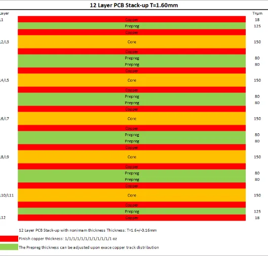
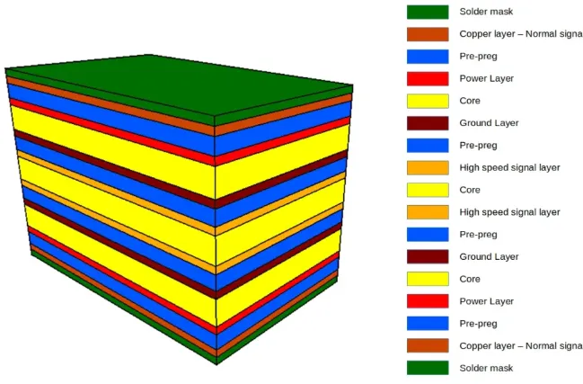
1. Plan Your Stack-Up Carefully
The foundation of a successful 12-layer PCB design lies in the stack-up. A typical configuration might include alternating signal and plane layers, such as:
- Layer 1: Top Signal
- Layer 2: Ground Plane
- Layer 3: Signal
- Layer 4: Power Plane
- ...and so on, with symmetry to minimize warping.
This arrangement ensures that each signal layer has a nearby reference plane for controlled impedance and reduced EMI. For high-speed designs, keep critical signals on inner layers to shield them from external noise.
2. Prioritize Signal Grouping and Separation
Group similar signals together to minimize interference. For example, keep high-speed digital signals away from sensitive analog traces. Use dedicated layers for critical nets, and maintain at least 3x the trace width as spacing between high-speed traces to reduce crosstalk. If a trace is 5 mils wide, aim for a 15-mil separation.
3. Optimize Via Usage
Vias are essential for connecting layers, but excessive use can introduce parasitic inductance and capacitance, degrading signal quality. Use microvias or buried vias for high-density areas to save space, and keep via stub lengths under 10 mils for signals above 1 GHz to avoid resonance issues.
4. Manage Power Distribution
Dedicate at least two layers to power and ground planes to ensure stable voltage delivery. Split power planes if you have multiple voltage levels (e.g., 3.3V and 5V), but avoid overlapping splits to prevent return path disruptions for signals crossing the split.
12-Layer PCB Routing Best Practices
Following 12-layer PCB routing best practices can make the difference between a functional design and one plagued by performance issues. Here are actionable tips to guide your process.
1. Start with a Schematic-Driven Design
Begin with a well-organized schematic that defines net names, component placement, and critical connections. This upfront planning reduces errors during routing and ensures that high-priority signals are addressed first.
2. Use 45-Degree Angles for Traces
Avoid sharp 90-degree corners in trace routing, as they can cause signal reflections and increase EMI. Instead, use 45-degree angles for smoother transitions. This is especially important for traces carrying signals faster than 500 MHz.
3. Maintain Consistent Trace Widths
For controlled impedance, keep trace widths consistent across a net. For a 50-ohm impedance line on a standard FR-4 material with a dielectric constant of 4.2, a trace width of around 6 mils on an outer layer might be needed (depending on layer thickness and stack-up). Use impedance calculators to verify these values.
4. Minimize Trace Lengths
Shorter traces reduce signal delay and loss. Route critical signals first, keeping their paths as direct as possible. For differential pairs, ensure equal lengths to maintain timing, with length mismatches under 5 mils for high-speed signals.
5. Implement Design Rule Checks (DRC)
Always run DRCs to catch spacing violations, unconnected nets, or manufacturing issues early. Set rules for minimum trace spacing (e.g., 5 mils) and via clearance to align with your manufacturer’s capabilities.
Choosing the Right 12-Layer PCB Routing Software
The complexity of a 12-layer design demands powerful 12-layer PCB routing software to streamline the process and minimize errors. Here’s what to look for in a tool and how it can help with 12-layer PCB routing density.
Key Features to Seek
- Advanced Autorouting: Look for software with intelligent autorouting capabilities that prioritize signal integrity and density while adhering to design rules.
- Impedance Control Tools: Built-in calculators for trace width and spacing ensure impedance matching for high-speed signals.
- 3D Visualization: This helps identify potential interference in dense layouts and verify layer stack-ups.
- Simulation Capabilities: Tools for signal integrity and thermal analysis can predict performance issues before fabrication.
- Design Rule Customization: Customizable DRCs ensure your design meets specific manufacturing constraints.
Using robust software tailored for multilayer designs can significantly reduce routing time and improve accuracy, especially for dense layouts with hundreds of components and thousands of connections.
Strategies for Managing 12-Layer PCB Routing Density
High 12-layer PCB routing density is a common hurdle in complex designs. Here are strategies to maximize space without compromising performance.
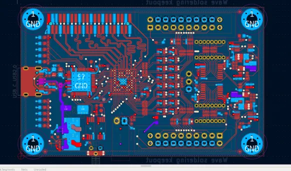
1. Optimize Component Placement
Place components strategically to minimize trace lengths and avoid congestion. Group related components together, and position high-speed ICs near their connectors to reduce signal travel distance.
2. Utilize Inner Layers Effectively
Route less critical or slower signals on outer layers, reserving inner layers for high-speed or noise-sensitive traces. This approach leverages the shielding provided by ground planes on adjacent layers.
3. Leverage Blind and Buried Vias
In dense areas, use blind and buried vias to connect layers without consuming surface space. For example, a blind via from layer 1 to layer 3 avoids drilling through the entire board, freeing up space on lower layers.
4. Fine-Tune Trace Spacing
In extremely dense areas, reduce trace spacing to the minimum allowed by your manufacturer (often 3-4 mils), but only if signal integrity isn’t compromised. Always simulate these changes to check for crosstalk risks.
Overcoming Common Pitfalls in 12-Layer PCB Routing
Even with the best tools and techniques, mistakes can happen. Here are common pitfalls in 12-layer PCB routing challenges and how to avoid them.
- Ignoring Return Paths: Ensure every signal has a continuous return path on an adjacent ground plane. Breaks in the return path can cause EMI spikes.
- Overloading Layers: Don’t cram too many traces on a single layer. Spread them across available layers to reduce congestion and maintain spacing.
- Neglecting Thermal Design: Add thermal vias under heat-generating components to transfer heat to inner layers or a heat sink. Aim for a via grid with 15-20 mils spacing for effective dissipation.
- Skipping Simulations: Always simulate your design for signal integrity and power distribution to catch issues like voltage drops or ringing before manufacturing.
Conclusion: Mastering 12-Layer PCB Routing
Routing a 12-layer PCB for dense and complex layouts is no small feat, but with the right approach, it’s a manageable and rewarding process. By applying the 12-layer PCB routing techniques and best practices outlined in this guide, leveraging powerful 12-layer PCB routing software, and addressing routing density and challenges head-on, you can achieve a design that balances performance, reliability, and manufacturability.
Start with a solid stack-up plan, prioritize signal integrity, and use every layer strategically to manage the complexity of your design. With careful attention to detail and the strategies shared here, your 12-layer PCB will be well-equipped to handle even the most demanding applications. Let this guide serve as your roadmap to success in multilayer PCB design.


