ALLPCB


In the fast-evolving world of electronics, multilayer printed circuit boards (PCBs) are the backbone of compact, high-performance devices like smartphones, medical equipment, and aerospace systems. At the heart of these intricate designs lies a seemingly simple yet critical component: the via. Vias are small, conductive pathways that connect different layers of a multilayer PCB, enabling complex routing and high-density circuitry. Without vias, the functionality and compactness of modern electronics would be severely limited. In this blog, we dive deep into the role of vias in multilayer PCB designs, exploring their types, applications, and best practices to help engineers optimize their projects.
What Are Vias in Multilayer PCBs?
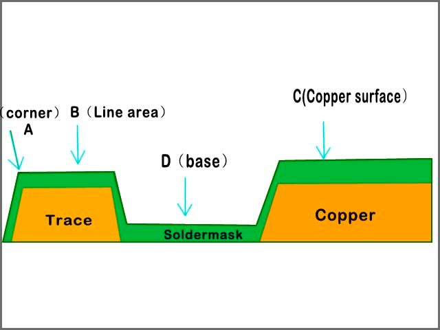
A via, short for Vertical Interconnect Access, is a small, plated hole that establishes electrical connections between different layers of a multilayer PCB. These holes are typically drilled or laser-cut through the PCB's laminate layers and plated with conductive materials like copper to facilitate the flow of electrical signals or power. Vias consist of three main parts: the barrel (the conductive tube inside the hole), the pad (a copper ring surrounding the hole on each layer), and the anti-pad (a clearance area isolating the via from other conductive elements).
Vias are indispensable in multilayer PCBs, which can have anywhere from four to over 100 layers, as they allow signals and power to traverse the board's thickness. This three-dimensional connectivity maximizes space efficiency, enabling designers to pack more functionality into smaller footprints. For example, a typical smartphone PCB might use thousands of vias to route high-speed signals across 8-12 layers, ensuring compact design without sacrificing performance.

Types of Vias in Multilayer PCB Designs
To meet diverse design requirements, vias come in several types, each suited to specific applications. Understanding these types is crucial for optimizing PCB performance and manufacturability.
Through-Hole Vias
Through-hole vias extend through the entire thickness of the PCB, connecting the top and bottom layers and any intermediate layers. They are the most common and cost-effective via type, widely used in designs where simplicity and reliability are priorities. For instance, a 4-layer PCB for an industrial control system might rely on through-hole vias to connect power and ground planes. However, their large size (typically 0.2-0.5 mm in diameter) can limit routing density in high-density interconnect (HDI) designs.
Blind Vias
Blind vias connect an outer layer (top or bottom) to one or more inner layers without passing through the entire board. These are ideal for HDI PCBs, where space is at a premium. For example, in a 10-layer PCB for a wearable device, blind vias might connect the top layer's microprocessor to an inner signal layer, freeing up surface space for other components. Blind vias require precise drilling depth control, increasing manufacturing complexity and cost.
Buried Vias
Buried vias connect two or more inner layers without reaching the outer surfaces, making them invisible from the top or bottom. They are used in advanced HDI designs to increase routing density. For instance, a 16-layer PCB for a telecommunications device might use buried vias to link internal signal layers, reducing surface congestion. Buried vias demand separate drill files and precise lamination, adding to fabrication costs.
Microvias
Microvias, with diameters less than 150 μm, are laser-drilled vias used in HDI PCBs for ultra-high-density routing. They often connect adjacent layers and can be stacked or staggered to form complex interconnects. In a modern laptop PCB, microvias might enable dense ball grid array (BGA) component connections, supporting high-speed signals up to 10 Gbps. Their small size enhances signal integrity but requires advanced manufacturing capabilities.

The Critical Roles of Vias in Multilayer PCBs
Vias are more than just connectors; they play multiple roles that directly impact a PCB's performance, reliability, and manufacturability. Below, we explore their key functions.
Enabling Inter-Layer Connectivity
The primary role of vias is to provide electrical pathways between layers, allowing signals and power to flow seamlessly. In a 6-layer PCB, for example, vias might connect a surface-mounted processor on the top layer to a power plane on layer 4 and a ground plane on layer 5. This connectivity is essential for complex circuits where surface routing alone is insufficient.
Enhancing Signal Integrity
Vias significantly influence signal integrity, especially in high-speed designs. Properly designed vias minimize impedance mismatches and signal distortion. For instance, in a PCB handling 5 GHz signals, microvias with controlled aspect ratios (typically 1:1 or less) reduce signal loss compared to larger through-hole vias. Ground vias placed near signal vias can also shield against electromagnetic interference (EMI), improving signal clarity.
Supporting Power Distribution
Vias connect power and ground planes across layers, ensuring efficient power delivery to components. In a 12-layer PCB for a server, multiple through-hole vias might link a power plane to a high-current component, maintaining a low-impedance path. Thermal vias, a specialized type, also dissipate heat from power-intensive components, enhancing reliability.
Optimizing Space and Routing Density
By enabling three-dimensional routing, vias reduce surface congestion, allowing designers to pack more traces and components into smaller areas. In HDI PCBs, microvias and buried vias can increase connection density by up to 50% compared to traditional designs, making them critical for compact devices like smartwatches.
Design Considerations for Vias in Multilayer PCBs
Effective via design requires careful planning to balance performance, cost, and manufacturability. Here are key considerations for engineers.
Via Size and Aspect Ratio
The via's diameter and aspect ratio (hole depth to diameter) affect both performance and fabrication. Smaller vias, like microvias with 0.1 mm diameters, support high-density routing but require precise laser drilling. A typical aspect ratio for through-hole vias is 10:1 (e.g., 2 mm board thickness with a 0.2 mm hole), while microvias aim for 1:1 to ensure reliability. Oversized vias waste space, while undersized ones risk incomplete plating.
Via Placement and Routing
Strategic via placement minimizes signal path lengths and EMI. For high-speed signals, vias should be placed close to components to reduce trace lengths, ideally under 10 mm for 3 GHz signals. Staggered or stacked microvias can optimize routing in HDI designs but increase costs. Designers should also avoid placing vias under sensitive components to prevent interference.
Impedance Control
Vias introduce impedance discontinuities that can degrade high-speed signals. To maintain controlled impedance (e.g., 50 ohms for RF signals), engineers can use ground vias or adjust via pad sizes. Simulation tools like Altium Designer or Cadence can model via impedance, ensuring signal integrity.
Manufacturability
Via types impact fabrication complexity. Through-hole vias are the easiest to manufacture, while blind and buried vias require multiple drilling and lamination steps, increasing costs by 20-30%. Microvias demand advanced laser drilling, which not all fabricators support. Engineers should consult with their PCB manufacturer early to align design choices with fabrication capabilities.

Challenges and Best Practices for Via Design
While vias are essential, they present challenges that engineers must address to ensure optimal PCB performance.
Challenges
- Signal Loss: High-frequency signals (above 1 GHz) can experience loss due to via stubs-unused portions of through-hole vias. For example, a 0.5 mm stub can cause a 3 dB signal loss at 10 GHz.
- Thermal Stress: Vias undergo thermal stress during soldering, risking barrel cracking. This is critical in thick boards (>2 mm) with high aspect ratio vias.
- Cost: Advanced vias like microvias or buried vias can increase fabrication costs by up to 50%, challenging budget-conscious projects.
- Fabrication Errors: Misaligned or incompletely plated vias can cause open circuits, with failure rates as high as 5% in complex HDI designs.
Best Practices
- Minimize Via Stubs: Use blind or buried vias to eliminate stubs in high-speed designs, or employ back-drilling to remove stubs post-fabrication.
- Optimize Layer Stackup: Design a balanced stackup with symmetrical layers to reduce warping and ensure via alignment. For a 10-layer PCB, a stackup with equal core and prepreg thicknesses (e.g., 0.1 mm each) is ideal.
- Use Simulation Tools: Simulate via performance using tools like Ansys HFSS to predict signal integrity and EMI before fabrication.
- Follow DFM Guidelines: Adhere to Design for Manufacturability (DFM) rules, such as maintaining a minimum annular ring size (e.g., 0.15 mm) for via pads to ensure reliable plating.
- Collaborate with Fabricators: Early consultation with your PCB manufacturer ensures via designs align with their equipment capabilities, reducing errors.

How ALLPCB Supports Advanced Via Designs
For engineers tackling complex multilayer PCB projects, partnering with a reliable manufacturer is crucial. We at ALLPCB offer state-of-the-art fabrication services tailored to advanced via designs, including HDI PCBs with microvias, blind, and buried vias. Our advanced laser drilling and electroplating technologies ensure precise via formation, supporting high-density interconnects with diameters as small as 0.1 mm. With over a decade of experience, we provide comprehensive design for manufacturability (DFM) checks to catch potential via-related issues early, ensuring high yield and reliability. Whether you're designing a 4-layer board for consumer electronics or a 20-layer PCB for aerospace, our team collaborates closely to deliver cost-effective, high-quality solutions that meet your exact specifications.
Conclusion
Vias are the unsung heroes of multilayer PCB designs, enabling the complex, compact, and high-performance circuits that power modern electronics. From through-hole vias in simple boards to microvias in cutting-edge HDI designs, these tiny connectors play critical roles in inter-layer connectivity, signal integrity, power distribution, and space optimization. By understanding via types, addressing design challenges, and following best practices, engineers can create reliable, high-performing PCBs that meet the demands of today's technology-driven world. With careful planning and collaboration with experienced manufacturers, vias can unlock the full potential of your multilayer PCB designs.