ALLPCB


For electrical engineers working on medical devices, pacemaker PCB miniaturization is a critical frontier. The push for ultra-small designs addresses the need for less invasive implants, improved patient comfort, and enhanced device functionality. However, shrinking PCB sizes introduces complex challenges like signal integrity, thermal management, and manufacturing limitations. In this blog, we explore these hurdles and provide practical solutions, focusing on technologies like high-density interconnects, microvias, component embedding, and thin-film innovations to achieve pacemaker PCB size reduction.
Whether you're designing the next generation of pacemakers or troubleshooting existing layouts, this guide offers actionable insights to help you navigate the intricacies of ultra-small PCB designs. Let’s dive into the challenges and cutting-edge solutions shaping the future of pacemaker technology.
Why Pacemaker PCB Miniaturization Matters
Pacemakers are life-saving devices that regulate heart rhythms, and their design has evolved significantly over the decades. Modern patients and healthcare providers demand smaller, lighter, and more efficient devices that minimize surgical impact and improve long-term wearability. For engineers, this means reducing the PCB footprint—often to dimensions as small as 1.5 cm2 or less—while maintaining reliability and performance.
Miniaturization also enables advanced features like wireless communication and longer battery life, which are critical for remote monitoring and reduced replacement surgeries. However, achieving pacemaker PCB size reduction isn’t just about scaling down; it requires innovative approaches to overcome spatial, electrical, and thermal constraints. Let’s break down the key challenges before exploring solutions.
Key Challenges in Pacemaker PCB Miniaturization
Designing ultra-small PCBs for pacemakers involves balancing size constraints with the need for high performance and safety. Here are the primary obstacles electrical engineers face:
1. Space Limitations and Component Density
Pacemaker PCBs must house microcontrollers, capacitors, resistors, and power management circuits in a confined space. As designs shrink, fitting these components without compromising functionality becomes a puzzle. For instance, a typical pacemaker circuit might require over 50 components, but the PCB area may be limited to under 2 cm2, forcing engineers to rethink traditional layouts.
2. Signal Integrity and Interference
With components packed closer together, the risk of electromagnetic interference (EMI) and crosstalk increases. High-frequency signals, often in the range of 1-10 MHz for sensing and pacing functions, can degrade if traces are too close or improperly shielded. Maintaining signal integrity in ultra-small designs is critical to ensure accurate heart rhythm detection and stimulation.
3. Thermal Management
Smaller PCBs have less surface area to dissipate heat, and pacemakers generate heat from power circuits and processing units. Overheating can damage components or harm surrounding tissue, with safe operating temperatures typically below 43°C for implantable devices. Engineers must address heat dissipation without adding bulky heat sinks that defeat the purpose of miniaturization.
4. Manufacturing and Assembly Constraints
Ultra-small designs often require advanced manufacturing techniques, such as microvia drilling or fine-pitch soldering, which can be costly and prone to defects. For example, a via diameter below 150 microns may be necessary, but not all manufacturers have the precision tools to achieve this consistently, leading to reliability issues.
5. Power Efficiency and Battery Constraints
Pacemakers rely on batteries with limited capacity due to size restrictions. A smaller PCB must still support low-power circuits to extend battery life—often targeting 10-15 years of operation. This demands ultra-efficient components and designs that minimize leakage currents, sometimes as low as 1-2 μA in standby mode.
Solutions for Ultra-Small Pacemaker PCB Designs
Despite these challenges, advancements in PCB technology offer viable solutions for pacemaker miniaturization. Below, we explore key strategies that electrical engineers can implement, focusing on our targeted long-tail keywords.
1. High-Density Interconnect (HDI) for Pacemakers
High-density interconnect (HDI) technology is a game-changer for pacemaker PCB size reduction. HDI allows for more connections in a smaller area by using finer traces (as narrow as 50 microns) and smaller vias. This enables multi-layer boards with up to 8-10 layers in a footprint of just 1-2 cm2, packing more functionality without increasing size.
For pacemakers, HDI reduces the board’s surface area while maintaining critical connections for sensing and pacing circuits. However, engineers must ensure proper impedance matching—often targeting 50 ohms for signal traces—to avoid reflection losses. HDI also requires advanced manufacturing, so partnering with specialized fabricators is essential.
Practical Tip: Use simulation tools like Altium Designer to model HDI layouts and predict EMI risks before fabrication. This can save costly redesigns, especially for trace widths below 75 microns.
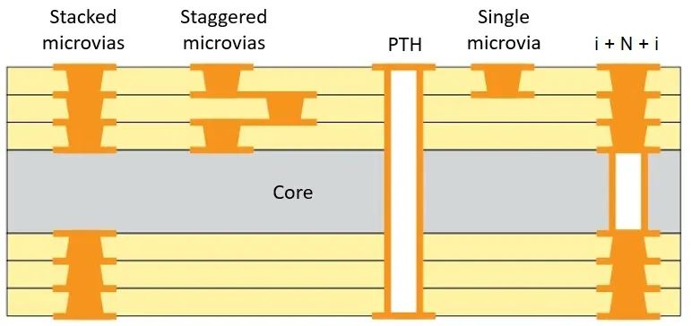
2. Microvia Technology in Pacemaker PCBs
Microvia technology complements HDI by enabling connections between layers through tiny, laser-drilled holes (typically under 150 microns in diameter). In pacemaker PCBs, microvias save space compared to traditional through-hole vias, allowing for denser component placement. For example, a board with microvias can reduce via-related spacing by 30-40%, freeing up area for additional circuitry.
However, microvias come with challenges like higher fabrication costs and potential reliability issues under thermal stress. Engineers should specify aspect ratios (depth-to-diameter) of 1:1 or lower to ensure plating integrity during manufacturing. Testing for via fatigue, especially under 200,000 strain cycles, is also crucial for long-term implant reliability.
3. Component Embedding for Pacemaker Miniaturization
Embedding components within the PCB substrate is a powerful technique for reducing surface area. Instead of mounting capacitors, resistors, or even ICs on the board’s surface, they are placed inside the layers, cutting the footprint by up to 50% in some designs. For pacemakers, this can mean embedding passive components like 1 μF capacitors directly under active chips, saving critical space.
Embedding also improves signal integrity by shortening interconnect lengths, reducing parasitic inductance by as much as 20-30 nH in high-frequency circuits. However, it requires precise lamination processes and can complicate repairs or testing. Engineers should prioritize embedding non-critical components first and use thermal vias to manage heat dissipation from embedded active parts.
Practical Tip: Work with PCB manufacturers who offer cavity embedding services, and validate designs with X-ray inspection to ensure component alignment within ±10 microns.
4. Thin-Film Technology for Pacemaker PCBs
Thin-film technology is an emerging solution for ultra-small pacemaker designs, enabling the creation of circuits with layers as thin as 1-2 microns. This approach uses deposition techniques to form conductive and insulating layers, ideal for flexible or rigid-flex PCBs that conform to the pacemaker’s housing. Thin-film traces can achieve resistances as low as 10 mΩ/cm, supporting efficient power delivery in compact layouts.
For pacemakers, thin-film technology reduces weight and thickness, sometimes bringing board profiles down to 0.1 mm. It’s particularly useful for integrating sensors directly into the PCB, enhancing functionality without adding bulk. However, thin-film processes are expensive and require specialized equipment, so cost-benefit analysis is critical for mass production.
Suggested Image Placement: Include an image here showing a thin-film PCB layer under a microscope, highlighting its ultra-thin structure. ALT Text: "Microscopic view of thin-film technology in pacemaker PCB for ultra-small designs."
5. Advanced Materials and Stack-Up Optimization
Beyond specific technologies, material selection plays a vital role in miniaturization. High-frequency laminates like Rogers RO4350B offer low dielectric constants (around 3.5) and loss tangents (0.0037 at 10 GHz), supporting signal integrity in dense layouts. Flexible substrates like polyimide also allow for bendable designs, fitting into irregular pacemaker shapes.
Optimizing the PCB stack-up is equally important. A 6-layer stack-up with alternating signal and ground planes can reduce EMI by 20-30% compared to a 4-layer design, even in a 1.5 cm2 board. Engineers should also consider blind and buried vias to maximize routing density without sacrificing reliability.
Practical Design Tips for Electrical Engineers
To successfully implement these solutions, consider the following actionable tips tailored for pacemaker PCB design:
- Simulate Early and Often: Use tools like SPICE or Ansys HFSS to model signal integrity and thermal performance before prototyping. For instance, ensure pacing signal rise times stay below 100 ns to avoid latency issues.
- Prioritize Power Planes: Dedicate at least one internal layer to a solid ground plane to minimize noise, targeting a loop inductance below 5 nH for critical circuits.
- Test for Biocompatibility: Ensure all materials and processes comply with ISO 10993 standards for implantable devices, especially for thin-film or embedded components exposed to body fluids.
- Collaborate with Fabricators: Engage with PCB manufacturers early to confirm capabilities for microvias or HDI, as tolerances below ±5 microns may not be universally supported.
Future Trends in Pacemaker PCB Miniaturization
The field of pacemaker design is evolving rapidly, and several trends promise to push miniaturization further. Wireless energy harvesting, as seen in recent studies, could eliminate bulky batteries, reducing PCB size by 20-30%. Bioresorbable materials, though still experimental, may enable temporary pacemakers that dissolve after use, requiring ultra-thin PCB designs with minimal footprints.
Additionally, advancements in 3D printing for PCBs could allow for custom, ultra-compact layouts tailored to individual patient anatomies. Engineers should stay updated on these developments, as they may redefine design constraints in the next 5-10 years.
Conclusion: Balancing Miniaturization with Reliability
Pacemaker PCB miniaturization is a complex but achievable goal for electrical engineers willing to embrace cutting-edge technologies like high-density interconnects, microvia technology, component embedding, and thin-film innovations. While challenges like signal integrity, thermal management, and manufacturing precision persist, the solutions outlined in this guide provide a roadmap for success.
By leveraging HDI for denser routing, microvias for space savings, and advanced materials for performance, engineers can design ultra-small pacemaker PCBs that meet the demands of modern healthcare. Start small with simulations, collaborate with experienced fabricators, and prioritize patient safety through rigorous testing. The future of pacemaker technology is compact, efficient, and life-changing—and it begins with your next design.