ALLPCB


If you're looking for practical tips on designing a 16-layer PCB with manufacturability in mind, you're in the right place. Designing for Manufacturability (DFM) for a 16-layer PCB involves adhering to specific guidelines like maintaining proper trace widths, clearances, drill sizes, and manufacturing tolerances to ensure a smooth production process and a reliable final product. In this comprehensive guide, we'll dive deep into the essential rules and best practices for 16-layer PCB DFM, covering everything from stack-up design to precise tolerances. Whether you're an experienced engineer or new to multilayer designs, this post will help you create PCBs that are both high-performing and easy to manufacture.
Why DFM Matters for 16-Layer PCBs
Designing a 16-layer PCB is no small task. These complex boards are often used in high-performance applications like telecommunications, aerospace, and advanced computing, where signal integrity and reliability are critical. However, without proper attention to Design for Manufacturability (DFM), even the best designs can face production delays, increased costs, or performance issues. DFM ensures that your 16-layer PCB design aligns with manufacturing capabilities, reducing errors and ensuring the board can be built efficiently.
By focusing on DFM early in the design process, you can avoid common pitfalls like unmanufacturable trace widths, improper clearances, or drill sizes that exceed standard tolerances. Let's break down the key guidelines to follow for a successful 16-layer PCB design.
Understanding the 16-Layer PCB Stack-Up
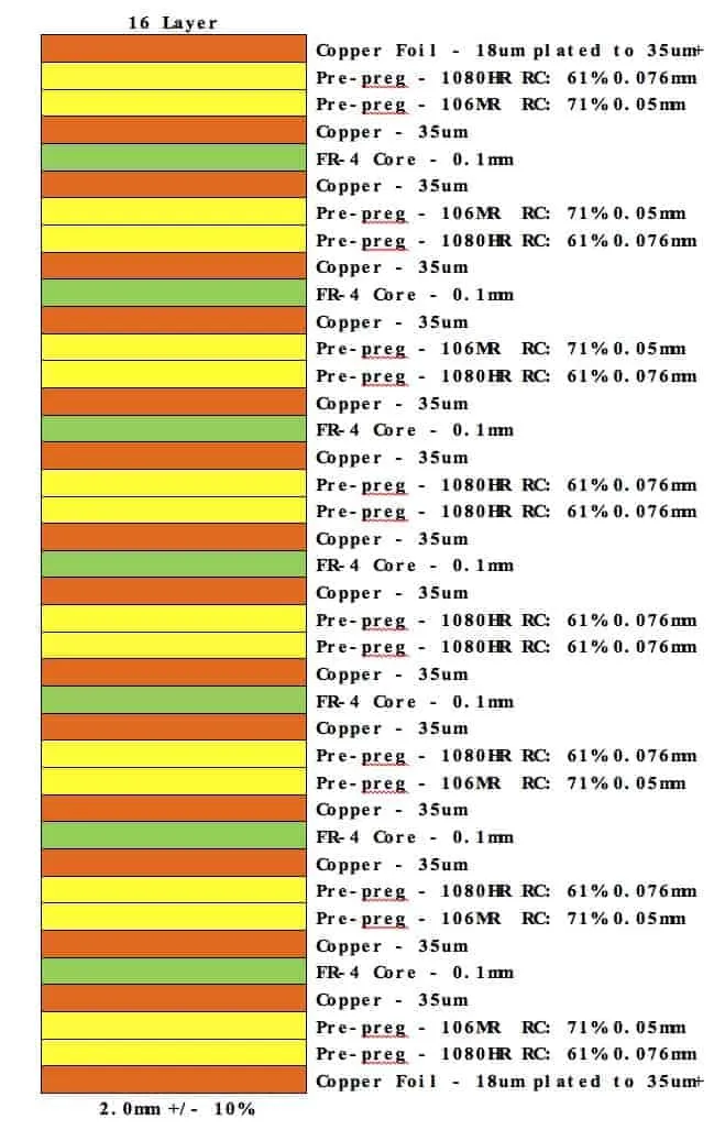
The foundation of any multilayer PCB design starts with the stack-up. For a 16-layer PCB, the stack-up defines how the signal, power, and ground layers are arranged to optimize signal integrity and thermal performance while meeting manufacturing constraints. A typical 16-layer stack-up might include multiple signal layers, dedicated ground planes, and power distribution layers, often arranged symmetrically to prevent warping during fabrication.
For DFM, ensure that your stack-up adheres to standard material thicknesses and dielectric constants. Most manufacturers prefer a balanced stack-up to avoid mechanical stress. For example, a common configuration might have ground planes on layers 2, 5, 8, 11, and 14, with signal layers in between and power planes strategically placed. Always consult with your fabrication partner to confirm material availability and layer spacing, as deviations can lead to production issues.
Additionally, keep impedance control in mind. High-speed signals on a 16-layer PCB often require controlled impedance traces, typically targeting values like 50 ohms for single-ended signals or 100 ohms for differential pairs. Use a stack-up calculator or simulation tool to verify these values based on your dielectric materials and trace geometries.
Key PCB Design Rules for 16-Layer DFM
Following strict PCB design rules is essential for ensuring your 16-layer board can be manufactured without issues. Below are the critical parameters to focus on, including trace width, clearance, and other design considerations.
1. Trace Width and Spacing
Trace width and spacing are crucial for maintaining signal integrity and preventing crosstalk in a 16-layer PCB. For high-density designs, trace widths often range from 4 to 6 mils (0.1 to 0.15 mm) for signal layers, depending on the current requirements and impedance needs. Power traces may need to be wider, sometimes up to 20 mils (0.5 mm) or more, to handle higher currents.
Spacing, or clearance, between traces should typically be at least 5 mils (0.13 mm) to avoid electrical interference and ensure manufacturability. For high-voltage applications, increase clearance to 8 mils (0.2 mm) or more, based on the voltage rating and safety standards. Always check with your manufacturer for their minimum trace width and spacing capabilities, as exceeding these limits can lead to etching defects or short circuits.
2. Drill Sizes and Via Design
Drilling is a critical step in PCB manufacturing, especially for a 16-layer board with numerous vias connecting layers. Standard drill sizes for through-hole vias typically start at 8 mils (0.2 mm), with aspect ratios (board thickness to drill diameter) ideally kept below 10:1 to ensure reliable plating. For a 16-layer PCB with a thickness of around 62 mils (1.6 mm), this means avoiding drill sizes smaller than 6 mils (0.15 mm) if possible.
For blind and buried vias, often used in multilayer designs to save space, work closely with your fabricator to confirm their capabilities. These vias require precise drilling and plating, and not all manufacturers support them for high-layer-count boards. Also, maintain an annular ring (the copper pad around the via) of at least 5 mils (0.13 mm) to ensure proper connection after drilling.
3. Manufacturing Tolerances
Manufacturing tolerances define the acceptable deviations in dimensions during PCB fabrication. For a 16-layer PCB, key tolerances to consider include:
- Board Thickness: Typically ±10% of the specified thickness, often around 62 mils (1.6 mm) for a 16-layer board.
- Drill Hole Size: ±2 mils (0.05 mm) for standard drills, though tighter tolerances may be available at a higher cost.
- Copper Thickness: Usually specified as 1 oz (35 μm) per layer, with a tolerance of ±10% after plating.
- Trace Width/Spacing: ±20% of the nominal value due to etching variations, so design with a buffer to account for this.
Designing within these tolerances ensures your board can be produced without costly reworks. Always review your fabricator's specific tolerance guidelines, as capabilities can vary.
Clearance and Layout Considerations
Clearance rules go beyond just trace spacing. For a 16-layer PCB, you must also consider clearance between components, pads, and board edges to prevent manufacturing defects. A minimum clearance of 10 mils (0.25 mm) between components and board edges is a good starting point, though this may increase for larger or heavier components to account for mechanical stress during assembly.
Additionally, ensure proper clearance around high-speed signal traces to minimize crosstalk. For differential pairs, maintain consistent spacing (often 5 to 8 mils or 0.13 to 0.2 mm) between the two traces and avoid routing them near noisy power lines. Use ground planes beneath signal layers to provide shielding and reduce electromagnetic interference (EMI).
Thermal and Power Distribution in 16-Layer PCBs
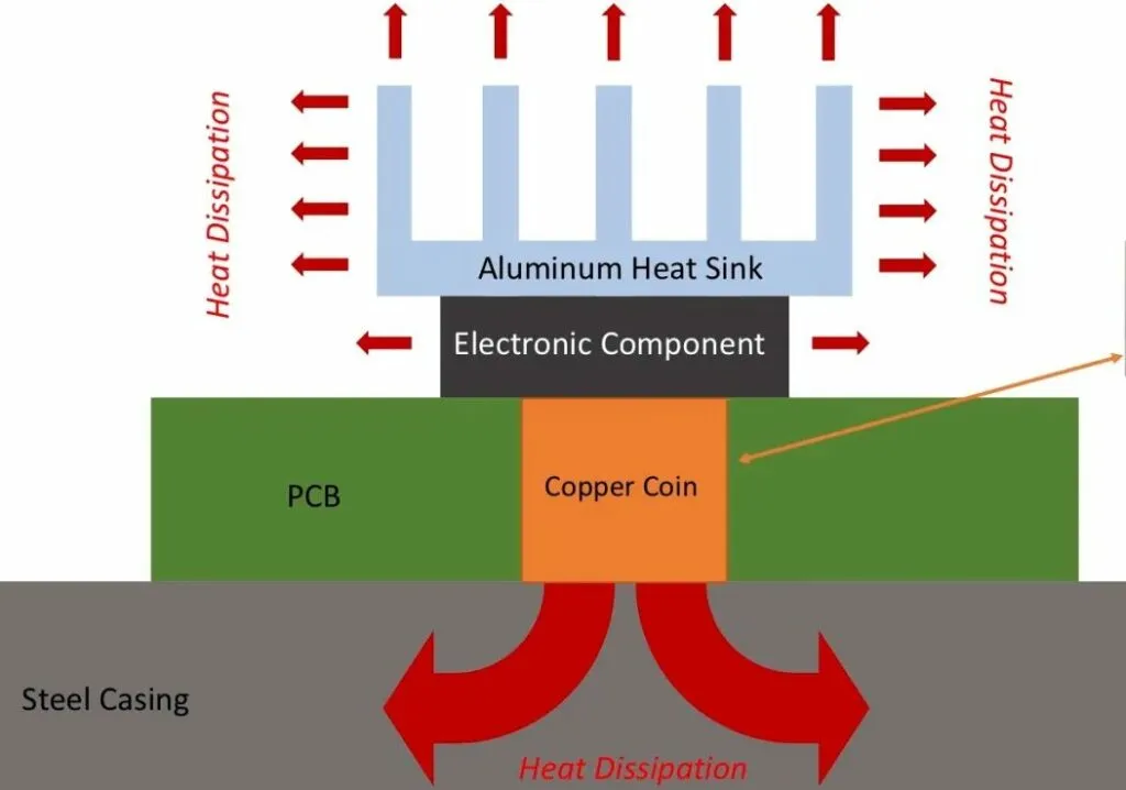
With so many layers, managing heat and power distribution becomes a significant concern. Dedicate internal layers to power and ground planes to ensure stable voltage delivery and minimize noise. For high-current applications, use thicker copper (e.g., 2 oz or 70 μm) on power layers to handle the load without overheating.
Thermal vias can help dissipate heat from hot components to inner layers or the opposite side of the board. Place these vias strategically near high-power components, with a diameter of at least 10 mils (0.25 mm) and a grid spacing of 40 mils (1 mm) for effective heat transfer. Simulation tools can help predict thermal performance and identify potential hotspots before manufacturing.
Material Selection for Manufacturability
Choosing the right materials is a cornerstone of DFM for 16-layer PCBs. Standard FR-4 material is often sufficient for many applications, with a dielectric constant (Dk) of around 4.2 to 4.5 at 1 MHz. However, for high-frequency designs, consider low-loss materials with a Dk of 3.0 to 3.5 to minimize signal attenuation.
Material thickness also affects manufacturability. Core and prepreg layers should align with standard thicknesses (e.g., 5 mils or 0.13 mm for cores) to avoid custom fabrication costs. Work with your manufacturer to select materials that balance performance and availability, as exotic materials can lead to longer lead times and higher expenses.
Testing and Validation for DFM
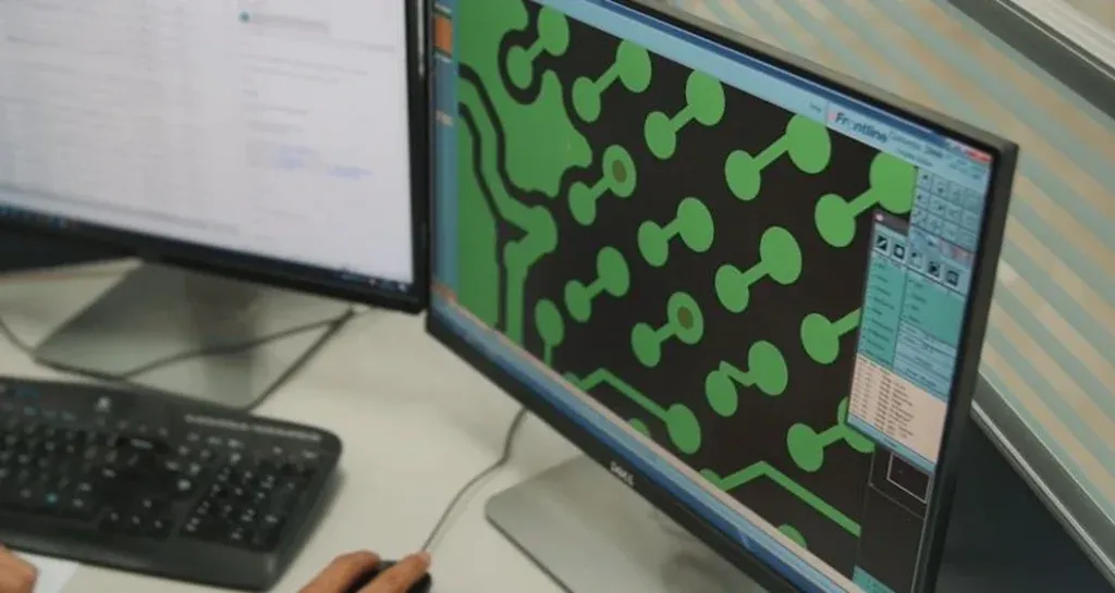
Before sending your 16-layer PCB design for fabrication, thorough testing and validation are essential. Use Design Rule Checking (DRC) tools to verify that your layout meets all specified tolerances, trace widths, and clearances. Additionally, simulate signal integrity to ensure that high-speed signals maintain their performance across layers.
For complex designs, consider ordering a prototype run to validate manufacturability. This step can uncover issues like misaligned vias or impedance mismatches that might not be apparent in simulations. Address any discrepancies before moving to full production to save time and resources.
Partnering with Your Manufacturer
One of the most important aspects of DFM for 16-layer PCBs is close collaboration with your fabrication partner. Early communication about your design requirements, including stack-up, tolerances, and special features like blind vias, can prevent misunderstandings and delays. Provide detailed documentation, including Gerber files, drill charts, and a Bill of Materials (BOM), to ensure clarity during production.
Many manufacturers offer DFM analysis services to review your design for potential issues. Take advantage of these services to refine your design and align it with their specific capabilities. A strong partnership can make the difference between a problematic build and a seamless production process.
Common Pitfalls to Avoid in 16-Layer PCB Design
Even with careful planning, certain mistakes can derail a 16-layer PCB project. Here are a few common pitfalls to watch out for:
- Ignoring Aspect Ratios: Using drill sizes that result in high aspect ratios can lead to plating failures in vias.
- Overlooking Symmetry: An unbalanced stack-up can cause warping during lamination, affecting the board's reliability.
- Inadequate Clearance: Insufficient spacing between traces or components can result in shorts or assembly issues.
- Neglecting Thermal Design: Failing to account for heat dissipation can cause component failure in high-power designs.
By addressing these potential issues during the design phase, you can significantly improve the manufacturability of your PCB.
Conclusion: Mastering 16-Layer PCB DFM
Designing a 16-layer PCB with manufacturability in mind requires careful attention to detail, from stack-up configuration to trace width, clearance, and manufacturing tolerances. By following the DFM guidelines outlined in this post—such as maintaining proper drill sizes, adhering to trace spacing rules, and selecting suitable materials—you can create a design that not only performs well but is also easy and cost-effective to produce.
Remember that every design is unique, so tailor these recommendations to your specific application and always collaborate with your fabrication partner for the best results. With a solid DFM approach, your 16-layer PCB will be ready to meet the demands of even the most complex projects, ensuring reliability and efficiency from design to delivery.