 ALLPCB


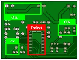
When it comes to ensuring the quality of printed circuit boards (PCBs), looking beyond the surface is critical. Hidden flaws in internal layers can lead to failures in electronic devices, costing time and money. So, how do you detect these unseen issues? Microsectioning is a powerful technique that reveals hidden PCB flaws by providing a detailed view of internal structures. Unlike non-destructive methods, it offers unmatched precision in identifying defects that could compromise performance. In this blog, we dive deep into microsectioning, compare it with other methods like X-ray inspection, and explore the limitations of non-destructive testing for PCB internal layers inspection. Let’s uncover the details that ensure your boards meet the highest standards.
What Are Hidden PCB Flaws and Why Do They Matter?
PCBs are complex, multi-layered structures that form the backbone of modern electronics. While surface-level defects like scratches or misaligned components are easy to spot, flaws hidden within internal layers—such as delamination, voids, or poor plating—can be far more dangerous. These issues may not be visible during initial testing but can cause signal loss, short circuits, or complete board failure over time.
For example, a void in the copper plating of a via might disrupt electrical connectivity, leading to intermittent failures. Similarly, delamination between layers can weaken the structural integrity of the board, especially under thermal stress. Detecting these flaws early through precise methods like microsectioning is essential for industries like aerospace, automotive, and medical, where reliability is non-negotiable.
What Is Microsectioning and How Does It Work?
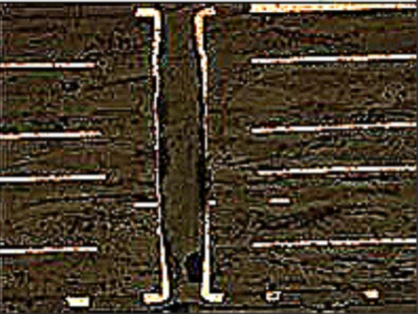
Microsectioning, also known as cross-sectioning, is a destructive testing method used for PCB internal layers inspection. It involves physically cutting a small section of the PCB, mounting it in a resin, and polishing it to create a smooth surface. This sample is then examined under a high-powered microscope to reveal the internal structure of the board.
The process typically follows these steps:
- Sample Preparation: A small piece of the PCB is cut using precision tools to avoid damaging the area of interest.
- Embedding: The sample is encased in epoxy resin to hold it in place during polishing.
- Polishing: The sample is ground and polished to expose a clean cross-section of the layers.
- Inspection: Using a microscope, engineers analyze the sample for defects such as cracks, voids, or improper layer alignment.
This method provides a direct view of the board’s internal features, including the thickness of copper layers (often measured in ounces per square foot, such as 1 oz or 2 oz), the quality of via plating, and the bonding between layers. For instance, microsectioning can detect if a via’s copper wall is too thin—below the typical 1 mil (0.001 inches)—which could lead to electrical failures under high current.
Microsectioning vs. X-Ray Inspection for PCB Testing
When comparing microsectioning vs. X-ray inspection for PCB testing, both methods have unique strengths and weaknesses. Understanding these differences helps engineers choose the right approach for their specific needs.
Microsectioning: Precision at a Cost
Microsectioning excels in providing detailed, high-resolution images of a PCB’s internal structure. It can detect minute defects, such as hairline cracks or incomplete plating in vias, that might be missed by other methods. For example, it can measure the exact thickness of dielectric layers—often between 4 to 8 mils in standard boards—and ensure they meet design specifications.
However, microsectioning is a destructive process. The tested sample cannot be reused, which can be a drawback for expensive or limited-production boards. It also requires skilled technicians and specialized equipment, adding to the cost and time involved.
X-Ray Inspection: Non-Destructive but Limited
X-ray inspection is a non-destructive testing method that uses radiation to penetrate the PCB and create images of its internal features. It’s ideal for detecting issues like misaligned layers or hidden solder defects in components like Ball Grid Arrays (BGAs). X-ray systems can often scan a board in minutes, making it faster than microsectioning.
However, X-ray inspection has limitations in resolution and detail. It may struggle to identify very small defects, such as thin cracks or subtle variations in material thickness. Additionally, interpreting X-ray images requires expertise, as overlapping layers can create confusing results.
In summary, microsectioning offers unmatched detail for critical applications where precision is key, while X-ray inspection is better suited for quick, non-destructive checks during production.
Non-Destructive PCB Testing Limitations
While non-destructive testing methods like X-ray inspection and automated optical inspection (AOI) are valuable for maintaining production efficiency, they come with significant limitations, especially for non-destructive PCB testing limitations in detecting internal flaws.
Limited Resolution and Depth
Non-destructive methods often lack the resolution needed to spot tiny defects. For instance, X-ray inspection might miss a crack in a via wall if it’s less than 0.5 mils wide. Similarly, AOI is limited to surface-level defects and cannot assess internal layers at all.
Inability to Measure Material Properties
Non-destructive testing struggles to evaluate material characteristics like the adhesion strength between layers or the exact thickness of copper plating. These properties are critical for ensuring a PCB can withstand thermal cycling or high-frequency signals (e.g., above 1 GHz, where impedance mismatches can degrade performance).
Interpretation Challenges
Images from non-destructive methods can be difficult to interpret, especially in complex multi-layer boards. Shadows or overlapping features in X-ray images might hide critical defects, leading to false negatives. This can be particularly problematic in high-density designs with 8 or more layers.
Due to these limitations, non-destructive methods are often used alongside destructive techniques like microsectioning for comprehensive quality control. While non-destructive testing saves time during production, it cannot replace the detailed insights provided by cutting and examining a board’s internal structure.
Key Benefits of Microsectioning for PCB Quality Control
Microsectioning stands out as a critical tool for ensuring PCB reliability, especially in high-stakes applications. Here are some of its primary advantages:
- Unmatched Detail: It reveals microscopic flaws, such as incomplete via fills or delamination, that could affect signal integrity (e.g., causing impedance variations beyond the acceptable ±10% tolerance).
- Material Analysis: Engineers can assess the quality of materials, like the uniformity of dielectric layers or the presence of contaminants, which impact long-term durability.
- Failure Analysis: When a PCB fails, microsectioning helps pinpoint the root cause, whether it’s a manufacturing defect or a design flaw.
- Standards Compliance: It ensures adherence to industry standards like IPC-6012, which specifies requirements for layer thickness and via quality.
For example, in a 6-layer PCB designed for high-speed applications, microsectioning might reveal that the inner copper layers are only 0.5 oz instead of the specified 1 oz, leading to potential overheating. Such insights are invaluable for preventing costly failures in the field.
When Should You Use Microsectioning?
Microsectioning is not needed for every PCB project due to its destructive nature and associated costs. However, it’s highly recommended in the following scenarios:
- Prototype Validation: During the design phase, microsectioning ensures that manufacturing processes meet specifications before mass production.
- High-Reliability Applications: For industries like medical or aerospace, where failure is not an option, microsectioning verifies internal quality.
- Failure Investigation: If a batch of boards fails during testing or in the field, microsectioning helps identify the cause, such as poor lamination or defective vias.
In contrast, for high-volume production with less stringent requirements, non-destructive methods like X-ray inspection might suffice for routine checks.
Best Practices for Effective Microsectioning
To get the most out of microsectioning, follow these best practices:
- Select Representative Samples: Choose sections of the PCB that are likely to show defects, such as areas near vias or high-stress points.
- Use Proper Tools: High-precision cutting and polishing equipment prevent damage to the sample, ensuring accurate results.
- Document Findings: Take detailed photographs and measurements during inspection to create a reference for future analysis.
- Combine with Other Tests: Use microsectioning alongside non-destructive methods to balance thoroughness with efficiency.
Conclusion: Going Beyond the Surface for PCB Excellence
Ensuring the quality of PCBs requires more than surface-level checks. Hidden flaws in internal layers can compromise performance, making thorough inspection methods essential. Microsectioning stands out as a powerful tool for PCB internal layers inspection, offering detailed insights that non-destructive methods like X-ray inspection often miss. While it’s a destructive process, its ability to reveal microscopic defects, validate material properties, and support failure analysis makes it indispensable for high-reliability applications.
Understanding the differences in microsectioning vs. X-ray inspection for PCB testing, as well as the non-destructive PCB testing limitations, allows engineers to choose the right approach for their needs. By incorporating microsectioning into your quality control process, you can catch hidden issues early, prevent costly failures, and deliver boards that meet the highest standards of performance and reliability.
At ALLPCB, we’re committed to helping you achieve excellence in every layer of your PCB. Whether you need detailed analysis through microsectioning or efficient non-destructive testing, our expertise and advanced tools ensure your boards are built to last.


