In the world of electronics manufacturing, ensuring high-quality printed circuit board (PCB) assembly is critical. One of the most effective tools for achieving this is Automated Optical Inspection (AOI), especially when it comes to managing solder paste application. So, how does AOI improve quality in solder paste processes? Simply put, AOI uses advanced cameras and imaging technology to detect defects like insufficient solder paste volume, misalignment, or solder joint issues early in the production line, ensuring better reliability and fewer failures.
In this blog, we’ll dive deep into the role of AOI in solder paste inspection, explore how it addresses common defects, and explain why it’s a game-changer for modern surface mount technology (SMT) assembly. Whether you’re an engineer or a manufacturer looking to optimize your production process, this guide will provide actionable insights into using AOI for superior quality control.
What Is Automated Optical Inspection (AOI) and Why Does It Matter?
Automated Optical Inspection, or AOI, is a non-contact testing method used in PCB manufacturing to visually inspect components and solder joints. By employing high-resolution cameras and sophisticated software, AOI systems scan PCBs to identify defects such as missing components, incorrect placements, or solder issues. This technology is widely used at various stages of production, including solder paste inspection, pre-reflow, and post-reflow checks.
The importance of AOI lies in its ability to catch errors early. For instance, in SMT assembly, up to 70% of defects can originate from improper solder paste application. By integrating AOI into the production line, manufacturers can reduce rework costs and improve product reliability. AOI is particularly vital for high-density boards where manual inspection is impractical due to tiny component sizes and tight tolerances.

The Role of Solder Paste in PCB Assembly
Solder paste is a crucial material in SMT assembly, acting as the adhesive that holds components in place before they are permanently bonded during the reflow process. It consists of tiny solder particles mixed with flux, which helps clean the surfaces for a strong connection. However, applying solder paste correctly is a delicate process. Too little paste can lead to weak joints, while too much can cause bridges or shorts between components.
Common issues with solder paste include uneven volume, misalignment on pads, and contamination. These problems can result in defective solder joints, which compromise the functionality and durability of the final product. This is where AOI steps in, offering a reliable way to inspect solder paste application before it’s too late.
How AOI Enhances Solder Paste Inspection
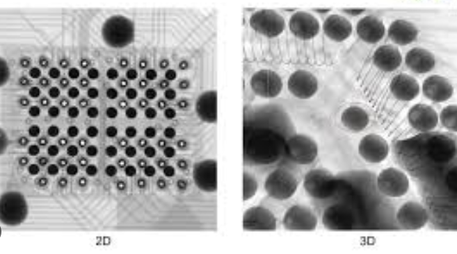
AOI plays a pivotal role in solder paste inspection (often referred to as SPI, or Solder Paste Inspection, when specifically focused on this stage). By using 2D and 3D imaging technologies, AOI systems measure critical parameters like solder paste volume, height, and area coverage on each pad. Here’s how AOI improves quality in this area:
- Accurate Volume Measurement: AOI can detect if the solder paste volume is within the acceptable range (typically between 80% and 120% of the target volume, depending on design specifications). Deviations outside this range can lead to weak or excessive joints.
- Alignment Verification: AOI ensures that solder paste is correctly aligned with the pads, preventing issues during component placement.
- Defect Detection: It identifies problems like smearing, insufficient paste, or contamination that could affect the soldering process.
By catching these issues early, AOI prevents defective boards from moving further down the production line, saving time and resources. For example, a study in electronics manufacturing found that implementing AOI at the solder paste stage reduced defect rates by up to 50% in high-volume production environments.

Addressing Solder Joint Defects with AOI
Solder joint defects are a leading cause of PCB failures, and AOI is uniquely equipped to tackle these issues. After the reflow process, AOI systems inspect the quality of solder joints to ensure they meet design standards. Common solder joint defects include:
- Solder Bridges: Excess solder connecting adjacent pads, causing short circuits.
- Insufficient Solder: Too little solder, resulting in weak or open connections.
- Tombstoning: Components standing on end due to uneven solder melting.
AOI uses high-resolution cameras to capture detailed images of each joint, comparing them against a database of acceptable standards. For instance, a typical AOI system can detect solder bridge defects as small as 50 micrometers, ensuring even the tiniest issues are flagged for correction. This precision is critical for modern electronics, where components are often smaller than 0.4 mm in size.
Moreover, 3D AOI systems take this a step further by providing depth information, allowing for more accurate detection of defects like insufficient solder height or joint shape irregularities. This technology ensures that even complex assemblies with high-density components are inspected with precision.

AOI Placement in the Production Line
The placement of AOI systems in the manufacturing process significantly impacts their effectiveness. AOI can be integrated at multiple stages, each serving a unique purpose:
- Post-Solder Paste Printing: At this stage, AOI focuses on solder paste volume and alignment, ensuring the foundation for component placement is solid. This early inspection can prevent up to 60% of potential defects before components are even placed.
- Pre-Reflow: AOI checks for component placement accuracy, ensuring parts are correctly positioned before soldering.
- Post-Reflow: This is the most common stage for AOI, where systems inspect solder joints for defects like bridges or insufficient solder after the board has been heated.
Strategically placing AOI at these points creates a multi-layered quality control system. For example, using AOI right after solder paste printing can catch issues before they escalate, while post-reflow inspection ensures the final product meets quality standards. Some advanced production lines even use real-time data from AOI to adjust upstream processes, like stencil printing settings, to minimize errors.
Benefits of Using AOI for Solder Paste and Joint Inspection
Integrating AOI into the PCB assembly process offers numerous advantages, especially when it comes to solder paste and joint quality. Here are some key benefits:
- Improved Accuracy: AOI systems provide consistent and precise inspections, far surpassing the capabilities of manual checks. They can detect defects as small as a few micrometers, ensuring high reliability.
- Cost Savings: By identifying issues early, AOI reduces the need for costly rework or scrap. For instance, fixing a solder paste issue before reflow is significantly cheaper than repairing a fully assembled board.
- Faster Production: AOI systems operate at high speeds, inspecting hundreds of pads per minute. This efficiency is crucial for high-volume manufacturing where delays can be costly.
- Enhanced Reliability: With AOI ensuring proper solder paste application and joint formation, the final product is more durable and less prone to failures in the field.
These benefits make AOI an indispensable tool for manufacturers aiming to maintain competitive quality standards in a fast-paced industry.
Challenges and Considerations in AOI for Solder Paste Inspection
While AOI offers significant advantages, it’s not without challenges. Understanding these limitations can help manufacturers use the technology more effectively:
- Complex Programming: Setting up AOI systems requires detailed programming to define acceptable parameters for solder paste volume and joint shapes. Incorrect settings can lead to false positives or missed defects.
- High Initial Costs: Advanced AOI equipment, especially 3D systems, can be expensive to purchase and install. However, the long-term savings from reduced defects often justify the investment.
- Limitations with Hidden Joints: For components like ball grid arrays (BGAs), AOI cannot inspect joints hidden beneath the package. In such cases, complementary technologies like X-ray inspection may be needed.
Despite these challenges, continuous advancements in AOI technology, such as machine learning algorithms, are improving accuracy and reducing setup times, making it an increasingly viable solution for all types of PCB assemblies.
Future Trends in AOI for Solder Paste Quality Control
The future of AOI in solder paste inspection looks promising, with several emerging trends set to enhance its capabilities:
- Artificial Intelligence Integration: AI-powered AOI systems are being developed to learn from past inspections, improving defect detection accuracy over time.
- Real-Time Process Control: Future AOI systems will provide immediate feedback to upstream equipment, automatically adjusting solder paste printing parameters to prevent recurring issues.
- Smaller Component Compatibility: As components continue to shrink, AOI systems are evolving to handle micro-scale inspections with resolutions down to a few micrometers.
These advancements will further solidify AOI’s role as a cornerstone of quality control in electronics manufacturing, ensuring that even the most complex assemblies meet stringent standards.
Conclusion: Elevating Quality with AOI and Solder Paste Inspection
In the fast-evolving field of PCB assembly, maintaining high quality is non-negotiable. Automated Optical Inspection (AOI) offers a powerful solution for ensuring the accuracy of solder paste application and the integrity of solder joints. By detecting issues like incorrect solder paste volume, misalignment, and joint defects early in the process, AOI helps manufacturers achieve reliable, defect-free products while saving time and costs.
From post-printing checks to post-reflow inspections, AOI’s strategic placement in the production line creates a robust quality control framework. As technology continues to advance, AOI will only become more precise and efficient, making it an essential tool for any modern electronics manufacturer.
By leveraging AOI for solder paste inspection and beyond, you can ensure that your assemblies meet the highest standards of quality and performance. Stay ahead in the industry by adopting this cutting-edge technology and watch your production process transform for the better.
 ALLPCB


