 ALLPCB


In the fast-paced world of electronics manufacturing, ensuring the quality and functionality of printed circuit boards (PCBs) is crucial. One of the most effective ways to achieve this is through In-Circuit Testing (ICT), a method that checks for defects like shorts, opens, and component failures directly on the board. However, to make ICT effective, your PCB design must be optimized for testability. This guide serves as a comprehensive handbook on design for testability ICT, offering practical tips and strategies to streamline your PCB layout for ICT fixtures. Whether you're focusing on ICT test point guidelines, PCB layout for ICT, test pad placement, or tooling holes for ICT fixtures, we’ve got you covered with actionable insights to improve your design process.
At ALLPCB, we understand the importance of creating testable designs that save time and reduce costs during production. In this blog, we'll dive deep into the principles of Design for Testability (DfT) and provide a step-by-step approach to optimizing your PCB for ICT fixtures. Let’s get started with the essentials and build toward advanced strategies to ensure your boards are ready for efficient testing.
What is ICT and Why Does Design for Testability Matter?
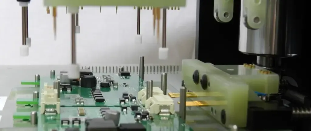
In-Circuit Testing (ICT) is a powerful testing method used in PCB manufacturing to detect manufacturing defects early in the production process. By using a specialized test fixture with probes, ICT checks individual components and connections on a fully assembled board without powering it up in most cases. This process identifies issues like incorrect component values, soldering defects, and short circuits, ensuring that only high-quality boards move forward in production.
However, the effectiveness of ICT heavily depends on how well your PCB is designed for testing. This is where design for testability ICT comes into play. A poorly designed PCB might lack accessible test points or have components placed in ways that obstruct probes, leading to incomplete testing or costly redesigns. By incorporating DfT principles from the start, you can minimize these risks, reduce testing time, and lower overall production costs. For instance, a well-optimized design can cut ICT setup time by up to 30%, according to industry studies, saving significant resources in high-volume production.
Key Principles of Design for Testability (DfT) in ICT
Design for Testability is a methodology that focuses on making your PCB easier to test during manufacturing. When applied to ICT, DfT ensures that your board layout supports efficient probe access, accurate testing, and minimal interference. Below are the core principles to follow for optimizing your PCB layout for ICT.
1. Plan Test Points Early in the Design Phase
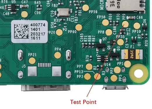
One of the most critical aspects of DfT is ensuring that there are enough test points on your PCB for ICT probes to access key nodes. Test points are small, exposed metal pads or vias where probes can make contact to measure signals or check connectivity. Without proper planning, you might end up with areas of the board that are untestable, leading to potential defects slipping through.
Here are some ICT test point guidelines to follow:
- Place test points on every net: Ideally, each electrical net (connection between components) should have at least one test point. This ensures comprehensive coverage during ICT.
- Size matters: Test pads should be large enough for reliable probe contact. A minimum diameter of 1.0 mm (40 mil) is often recommended, though 1.5 mm (60 mil) is better for high-density boards.
- Spacing is key: Keep test points at least 2.5 mm (100 mil) apart to avoid probe interference. This spacing allows for accurate targeting without risking damage to neighboring points.
- Accessibility: Place test points on the bottom side of the PCB whenever possible, as most ICT fixtures probe from below. Avoid placing them under large components or in areas blocked by heat sinks or connectors.
By adhering to these guidelines, you can ensure that your design supports thorough testing and reduces the chances of missed defects.
2. Optimize Test Pad Placement for Probe Access
Effective test pad placement goes hand-in-hand with test point planning. Poorly placed pads can result in probes missing their targets or causing mechanical stress on the board. Here are some best practices:
- Uniform grid alignment: Arrange test pads in a grid pattern if possible. Many ICT fixtures are designed to work with a standard grid spacing (e.g., 2.54 mm or 100 mil), which simplifies fixture design and reduces costs.
- Avoid edges: Don’t place test pads too close to the board’s edges (keep at least 3 mm clearance) to prevent probe misalignment during testing.
- Clear markings: Label test points clearly in your design files with silkscreen markings. This helps during fixture setup and troubleshooting if issues arise.
Proper placement not only improves test accuracy but also extends the lifespan of the ICT fixture by reducing wear on probes due to misalignment.
3. Incorporate Tooling Holes for ICT Fixtures
Another crucial element of optimizing your design is the inclusion of tooling holes for ICT fixtures. These holes are used to precisely align the PCB within ICT test fixtures, ensuring that probes make accurate contact with test points. Without proper alignment, even the best-designed test points can become ineffective.
Consider these tips for tooling holes:
- Number and placement: Use at least two tooling holes, ideally three, placed on opposite diagonal corners of the PCB. This ensures stable positioning and minimizes rotational errors.
- Non-plated holes: Tooling holes should not be plated to maintain dimensional accuracy. Plating can introduce slight variations that affect alignment.
- Size and tolerance: A common diameter for tooling holes is 3.175 mm (125 mil), with a tight tolerance of ±0.05 mm to ensure precise fit with fixture pins.
By carefully designing tooling holes, you can significantly improve the repeatability and accuracy of ICT, especially for high-volume production runs.

4. Simplify Component Placement for Accessibility
Component placement directly impacts the ease of ICT. Crowded layouts or components placed over test points can block probe access, making testing difficult or impossible. Follow these tips for a test-friendly PCB layout for ICT:
- Keep components away from test points: Maintain a clearance of at least 2 mm around test pads to avoid interference from tall components like capacitors or connectors.
- Standardize component orientation: Align components in a consistent direction to simplify fixture design and reduce the risk of probe collisions.
- Minimize bottom-side components: Since ICT probes typically access the board from the bottom, limit components on this side to essential ones only, and ensure they don’t obstruct test points.
These steps help create a layout that supports efficient testing without compromising the board’s functionality.
Advanced Strategies for ICT Optimization
Beyond the basics, there are advanced techniques you can apply to further enhance your PCB’s testability. These strategies are particularly useful for complex or high-density designs where standard DfT practices might not suffice.
1. Use Test-Specific Layers in Design Software
Modern PCB design softwares allow you to create dedicated layers for test points and annotations. By separating test-related elements into their own layer, you can easily share this information with your manufacturing and testing teams. This reduces errors during fixture design and ensures that all test points are accounted for. For example, you can set impedance values for critical nets (e.g., 50 ohms for high-speed signals) and ensure test points are placed to verify these parameters during ICT.
2. Simulate Probe Contact During Design
Before finalizing your layout, simulate the ICT process using design software or by consulting with your testing team. Check for potential probe interference, especially in dense areas of the board. Some tools can even model probe spring force (typically 100-200 grams per probe) to ensure test pads can withstand repeated contact without damage.
3. Balance Test Coverage with Cost
While it’s ideal to have a test point on every net, this isn’t always cost-effective for large or complex boards. Prioritize test points for critical nets, such as power lines or high-speed signals (e.g., signals above 100 MHz), where defects could cause significant issues. Work with your testing team to determine the minimum test coverage needed—often 85-90% of nets is a practical target for most projects.
Common Pitfalls to Avoid in ICT Design
Even with the best intentions, certain design mistakes can undermine your efforts to create a testable PCB. Here are some common pitfalls to watch out for:
- Ignoring fixture constraints: Not all ICT fixtures support the same probe spacing or board sizes. Confirm the capabilities of your testing setup before finalizing your design.
- Overlooking silkscreen clarity: Unclear or missing labels for test points can lead to confusion during fixture setup, increasing setup time by up to 20%.
- Neglecting mechanical stress: Repeated probe contact can stress small test pads or vias. Ensure pads are reinforced with adequate copper thickness (e.g., 1 oz or 35 μm) to prevent cracking.
Benefits of Optimizing PCB Design for ICT
Investing time in optimizing your PCB for ICT yields significant benefits throughout the manufacturing process. Here are just a few advantages:
- Higher defect detection rates: A well-designed board can achieve up to 95% defect detection during ICT, reducing the risk of faulty products reaching customers.
- Reduced testing costs: Efficient designs cut down on fixture setup time and minimize the need for manual testing, saving up to 15-25% on testing expenses.
- Faster time-to-market: Streamlined testing processes mean quicker production cycles, helping you meet tight deadlines without sacrificing quality.
Conclusion: Building Testability into Every Design
Optimizing your PCB design for ICT test fixtures is not just a best practice—it’s a necessity for ensuring quality and efficiency in electronics manufacturing. By focusing on design for testability ICT, adhering to ICT test point guidelines, refining your PCB layout for ICT, ensuring proper test pad placement, and incorporating tooling holes for ICT fixtures, you can create boards that are easier to test and more reliable in the long run.


