 ALLPCB


Designing printed circuit boards (PCBs) for navigation systems can be a complex and costly process, but with the right strategies, you can achieve significant savings without compromising on quality or performance. Whether you're working on GPS devices, automotive navigation units, or marine tracking systems, optimizing your design for cost and manufacturability is key. In this comprehensive guide, we'll explore proven methods for navigation PCB cost optimization, including tips on navigation PCB component selection, navigation PCB layer count, navigation PCB manufacturing process, and navigation PCB design for manufacturability. Let's dive into actionable strategies that can help you reduce costs while maintaining reliability and efficiency.
Why Cost Optimization Matters for Navigation System PCBs
Navigation systems are integral to industries like automotive, aerospace, and consumer electronics, where precision and reliability are non-negotiable. However, the high complexity of these systems often leads to elevated production costs due to intricate designs, specialized components, and stringent performance requirements. By focusing on cost-effective design practices, you can lower expenses during prototyping and mass production, making your products more competitive in the market. The strategies we'll cover not only help save money but also improve the overall manufacturability of your PCBs, reducing errors and delays in production.
1. Navigation PCB Cost Optimization: Start with a Budget-Friendly Mindset
The foundation of cost optimization begins at the design stage. Every decision, from material selection to layout planning, impacts the final production cost. Here are some essential tips for keeping expenses in check:
- Minimize Board Size: Smaller PCBs use less material and are cheaper to manufacture. Aim to design compact layouts without sacrificing functionality. For instance, a typical navigation PCB for a handheld GPS device might measure 50mm x 30mm, significantly reducing material costs compared to larger boards.
- Use Standard Materials: Opt for widely available PCB materials like FR-4, which is cost-effective and suitable for most navigation systems operating at frequencies below 1 GHz. Avoid exotic materials unless high-frequency performance (above 5 GHz) is critical.
- Plan for Volume Production: Design with scalability in mind. For example, panelizing multiple PCBs on a single sheet during manufacturing can reduce per-unit costs by up to 30%, especially for high-volume orders.
By adopting these practices early, you can avoid costly redesigns and ensure your navigation PCB remains budget-friendly throughout its lifecycle.
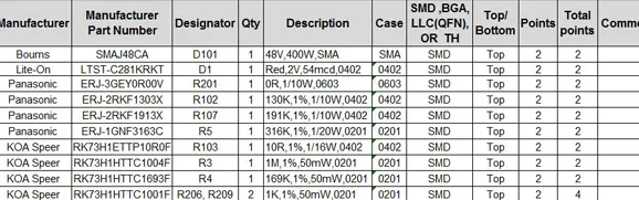
2. Navigation PCB Component Selection: Choose Wisely to Save Costs
Component selection plays a major role in both cost and performance of navigation system PCBs. These systems often require microcontrollers, RF modules, antennas, and sensors, which can quickly add up in price. Follow these guidelines to make cost-effective choices:
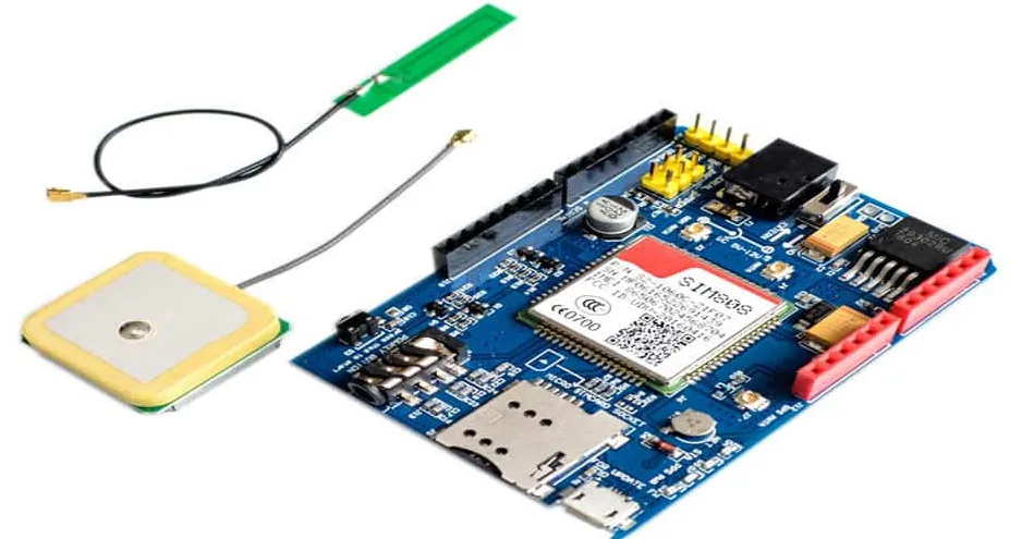
- Prioritize Generic Components: Whenever possible, use off-the-shelf components instead of custom parts. For example, a standard GPS module with a sensitivity of -165 dBm can often meet navigation requirements at a fraction of the cost of a custom-designed solution.
- Reduce Component Count: Simplify your design by integrating functions into fewer components. For instance, choose a microcontroller with built-in analog-to-digital converters (ADCs) to eliminate the need for separate ADC chips.
- Source from Multiple Suppliers: Avoid dependency on a single supplier by selecting components available from multiple sources. This prevents price spikes due to supply chain disruptions.
Additionally, consider the long-term availability of components. Using parts with a high risk of obsolescence can lead to redesign costs down the line. Always check datasheets and lifecycle status before finalizing your bill of materials (BOM).
3. Navigation PCB Layer Count: Balance Performance and Cost
The number of layers in a PCB directly affects manufacturing costs. Navigation systems often require multilayer boards to accommodate complex circuitry, but adding layers increases expenses. Here's how to optimize navigation PCB layer count:
- Assess Signal Integrity Needs: Navigation systems typically handle high-frequency signals for GPS and RF communication. A 4-layer board is often sufficient for separating power, ground, and signal planes, ensuring impedance control at 50 ohms for RF traces.
- Avoid Over-Engineering: Don’t default to a 6 or 8-layer board unless your design demands it. For example, if your navigation system operates below 2 GHz and doesn’t require advanced shielding, a 4-layer PCB can save up to 20% in production costs compared to a 6-layer design.
- Use Simulation Tools: Run simulations to verify signal integrity and electromagnetic interference (EMI) performance before increasing layer count. This helps confirm whether additional layers are truly necessary.
By carefully evaluating your layer requirements, you can avoid unnecessary expenses while maintaining the performance needed for accurate navigation data processing.
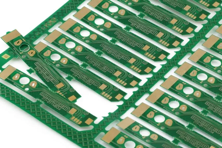
4. Navigation PCB Manufacturing Process: Streamline for Efficiency
The navigation PCB manufacturing process is another area where costs can be controlled through smart planning. Manufacturing inefficiencies often lead to delays and added expenses, so focus on these strategies:
- Panelization for Bulk Production: As mentioned earlier, grouping multiple PCBs on a single panel reduces material waste and lowers per-unit costs. Ensure your design adheres to standard panel sizes (e.g., 18” x 24”) to maximize efficiency.
- Simplify Assembly Requirements: Use surface-mount technology (SMT) components instead of through-hole parts where possible. SMT assembly is faster and cheaper, especially for high-density navigation PCBs with numerous small components.
- Minimize Manual Processes: Avoid designs that require manual soldering or custom fixtures. Automated assembly lines are far more cost-effective for producing navigation systems at scale.
Collaboration with your manufacturing partner is also critical. Share your design files early to get feedback on potential cost-saving adjustments before production begins. This proactive approach can prevent expensive errors during the navigation PCB manufacturing process.
5. Navigation PCB Design for Manufacturability: Build with Production in Mind
Designing for manufacturability (DFM) ensures that your navigation PCB can be produced efficiently with minimal errors. Poor DFM practices can lead to rework, delays, and higher costs. Here are key tips for navigation PCB design for manufacturability:
- Adhere to Design Rules: Follow standard design rules for trace width, spacing, and via sizes. For instance, maintain a minimum trace width of 6 mils and spacing of 6 mils for standard manufacturing processes to avoid fabrication issues.
- Optimize Component Placement: Place components logically to minimize trace lengths and reduce EMI. For navigation systems, position RF components like GPS antennas away from noisy power circuits to maintain signal integrity.
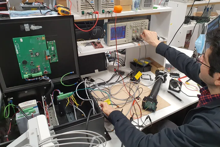
- Include Test Points: Add test points in your design to facilitate quality control during manufacturing. This reduces the risk of defective boards reaching the market, saving costs on returns and repairs.
- Avoid Tight Tolerances: Unless absolutely necessary, don’t specify extremely tight tolerances for drilling or etching. Standard tolerances (e.g., ±0.1mm for drill holes) are cheaper and easier to achieve.
By incorporating DFM principles, you can streamline production, reduce waste, and lower costs while ensuring your navigation PCB meets performance standards.
6. Additional Tips for Reducing Costs in Navigation PCB Design
Beyond the core strategies, there are other ways to achieve cost savings in navigation PCB projects. These tips focus on long-term planning and collaboration:
- Leverage Open-Source Tools: Use free or low-cost design software to create and simulate your PCB layouts. This cuts down on upfront costs without sacrificing design quality.
- Prototype Before Mass Production: Build and test a small batch of prototypes to identify design flaws early. Fixing issues during prototyping is far cheaper than addressing them after full-scale production.
- Work Closely with Manufacturers: Establish a strong relationship with your PCB fabrication and assembly partners. Their expertise can guide you toward cost-saving design adjustments specific to their capabilities.
Implementing these additional measures can further enhance your navigation PCB cost optimization efforts, ensuring a smoother path from design to market.
Conclusion: Achieve Cost-Effective Navigation PCBs with Smart Design
Designing cost-effective PCBs for navigation systems doesn’t mean cutting corners or sacrificing quality. By focusing on navigation PCB cost optimization, making informed decisions during navigation PCB component selection, balancing navigation PCB layer count, streamlining the navigation PCB manufacturing process, and prioritizing navigation PCB design for manufacturability, you can significantly reduce expenses while delivering reliable, high-performance products. Start with a budget-conscious mindset, collaborate with manufacturing partners, and use the tips outlined in this guide to optimize every stage of your PCB development.
At ALLPCB, we’re committed to helping engineers and designers bring their navigation system projects to life with affordable, high-quality PCB solutions. Apply these strategies in your next project to see the difference in both cost and efficiency. With careful planning and execution, you can create navigation PCBs that meet industry standards without breaking the bank.


