 ALLPCB


If you're looking to create precise and efficient double-sided SMT assemblies, designing laser cut stencils is a critical step. These stencils ensure accurate solder paste application, which is the foundation of a successful surface mount technology (SMT) assembly process. In this comprehensive guide, we'll walk you through the entire process of designing laser cut stencils for double-sided PCBs, covering topics like stencil alignment fiducials, solder paste application techniques, and the overall SMT assembly process. Whether you're a seasoned engineer or new to PCB design, this step-by-step tutorial will help you achieve high-quality results.
Why Laser Cut Stencils Matter for Double-Sided PCB Assembly
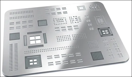
Laser cut stencils are essential tools in modern electronics manufacturing, especially for double-sided PCBs where components are mounted on both sides of the board. These stencils, made with precision laser cutting technology, allow for accurate deposition of solder paste onto the PCB pads before component placement. Unlike traditional etched stencils, laser cut stencils offer smoother edges and tighter tolerances, often achieving accuracy within ±5 microns. This precision is vital for fine-pitch components like 0.4mm QFPs or 0201 chip resistors, commonly found in compact double-sided designs.
For double-sided assemblies, the challenge lies in applying solder paste to both sides without misalignment or defects. A well-designed stencil ensures consistent paste volume, reducing issues like bridging or insufficient solder joints during the reflow process. By investing time in proper stencil design, you can significantly improve assembly yield and product reliability.
Understanding Double-Sided SMT Assembly Challenges
Double-sided SMT assemblies present unique challenges compared to single-sided boards. Since components are placed on both the top and bottom layers, the assembly process requires two separate solder paste applications and reflow cycles. This doubles the risk of misalignment, uneven paste distribution, and component displacement. Additionally, thermal stress from multiple reflows can cause board warping if not managed properly.
To address these issues, stencil design must account for precise alignment, appropriate aperture sizing, and compatibility with the reflow process. Fiducial marks, which we'll discuss later, play a key role in ensuring alignment during paste application on both sides. Let’s dive into the step-by-step process of designing laser cut stencils tailored for double-sided SMT assemblies.
Step 1: Prepare Your PCB Design for Stencil Creation
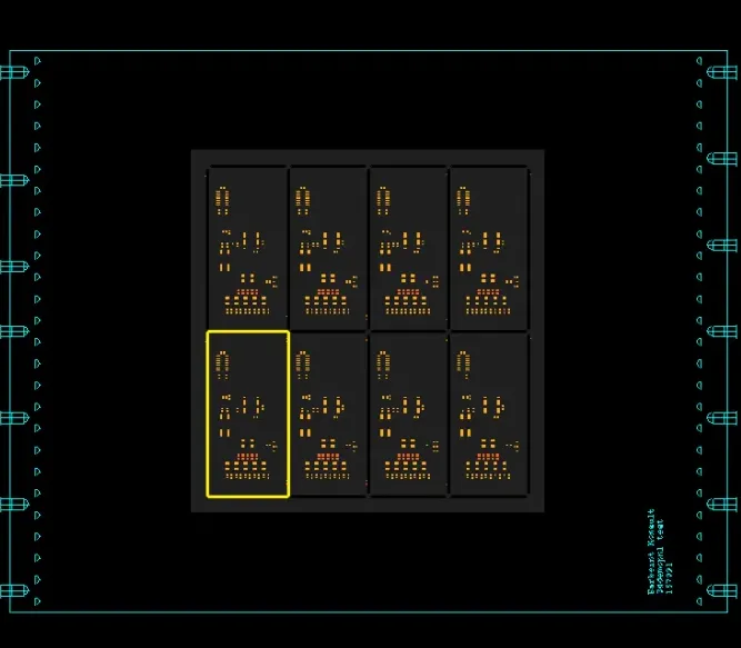
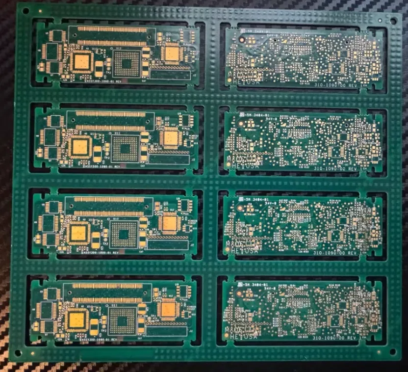
The first step in designing a laser cut stencil for a double-sided PCB is to finalize your PCB layout. Ensure that your design files include separate Gerber layers for the top and bottom solder paste masks. These layers define where the solder paste will be applied and are used to generate the stencil apertures.
Pay attention to component pad sizes and spacing. For fine-pitch components (e.g., pads spaced less than 0.5mm apart), you may need to reduce the aperture size by 10-15% to prevent excess paste and potential bridging. For larger pads, like those for power components, a 1:1 ratio with the pad size often works well. Most PCB design software allows you to export these paste mask layers directly for stencil fabrication.
Additionally, verify that your design includes fiducial marks—small reference points on the PCB used for alignment during stencil printing and component placement. We’ll cover fiducials in more detail in a later section.
Step 2: Choose the Right Stencil Material and Thickness
Selecting the appropriate material and thickness for your laser cut stencil is crucial for achieving consistent solder paste application. Most stencils are made from stainless steel due to its durability and resistance to wear. Stainless steel stencils can withstand thousands of print cycles, making them ideal for both prototyping and production runs.
Stencil thickness typically ranges from 0.1mm to 0.2mm, depending on the component types and paste volume required. For double-sided PCBs with mixed components, consider the following guidelines:
- 0.1mm (4 mil): Suitable for ultra-fine pitch components (e.g., 0.4mm pitch or smaller) where minimal paste volume is needed.
- 0.12-0.15mm (5-6 mil): A versatile choice for most standard SMT components, balancing paste volume and precision.
- 0.2mm (8 mil): Used for larger components or connectors requiring more solder paste.
For double-sided assemblies, you may need two stencils—one for each side—if the component mix and paste requirements differ significantly between layers. However, if the paste requirements are similar, a single stencil with flipped orientation can sometimes be used with careful alignment.
Step 3: Incorporate Stencil Alignment Fiducials
Alignment is a critical factor in double-sided SMT assembly, and fiducial marks are the key to ensuring precision. Fiducials are small, non-functional copper marks (typically 1-2mm in diameter) placed on the PCB and mirrored on the stencil. They act as reference points for aligning the stencil with the PCB during solder paste printing.
For double-sided PCBs, include at least three fiducial marks on each side, ideally positioned near the corners of the board in a triangular pattern. This configuration allows for accurate rotational and translational alignment. Ensure the fiducials on the stencil match the PCB exactly, as even a 0.05mm mismatch can lead to paste misalignment, especially on fine-pitch components.
Modern stencil printing machines use vision systems to detect fiducials automatically, so consistency between your PCB and stencil design files is essential. If you're working manually or with a desktop printer, take extra care to align the stencil using these marks before applying paste.
Step 4: Design Apertures for Optimal Solder Paste Application
The apertures (openings) in your laser cut stencil determine how much solder paste is deposited on each pad. For double-sided assemblies, aperture design must balance the needs of both sides while preventing common defects like bridging or insufficient solder.
Here are some solder paste application techniques and design tips for apertures:
- Aperture Reduction: For fine-pitch components, reduce the aperture size by 10-20% compared to the pad size to control paste volume. For example, a 0.5mm x 0.3mm pad might have a 0.45mm x 0.25mm aperture.
- Aspect Ratio: Maintain an aspect ratio (aperture width to stencil thickness) of at least 1.5 to ensure proper paste release. For a 0.15mm thick stencil, the smallest aperture width should be at least 0.225mm.
- Tapered Edges: Laser cut stencils often feature slightly tapered aperture walls (wider at the top), which aids in paste release and reduces clogging during printing.
For double-sided PCBs, test your stencil design with a small batch to confirm paste application consistency on both sides. Adjust aperture sizes if you notice uneven deposits or defects after the first reflow.
Step 5: Fabricate Your Laser Cut Stencil
Once your stencil design is ready, it’s time to fabricate it using laser cutting technology. Laser cutting offers unmatched precision, creating apertures with smooth edges and tolerances as tight as ±0.005mm. This is especially important for double-sided assemblies where even minor deviations can lead to assembly failures.
Work with a trusted stencil manufacturer to ensure high-quality results. Provide them with your Gerber files for the top and bottom paste layers, along with any specific instructions for thickness or material. Many manufacturers offer quick-turn services, delivering stencils within 24-48 hours for urgent projects.
Step 6: Master the SMT Assembly Process for Double-Sided Boards
With your laser cut stencils ready, you can proceed to the SMT assembly process. Double-sided assembly typically follows these steps:
- Solder Paste Application (Top Side): Align the stencil with the top side of the PCB using fiducials. Use a squeegee to apply solder paste evenly across the stencil, ensuring all apertures are filled. Remove the stencil carefully to avoid smearing.
- Component Placement (Top Side): Place components on the top side using a pick-and-place machine or manually for small runs. Ensure precise alignment with the solder paste deposits.
- First Reflow: Pass the PCB through a reflow oven to melt the solder paste and secure components on the top side. Use a reflow profile suited to your solder paste type (e.g., lead-free profiles typically peak at 245°C for 30-60 seconds).
- Solder Paste Application (Bottom Side): Flip the PCB and repeat the stencil alignment and paste application process for the bottom side. Be cautious, as the top-side components are now soldered and can shift if mishandled.
- Component Placement (Bottom Side): Place components on the bottom side. For heavier components, consider using adhesive dots to prevent displacement during the second reflow.
- Second Reflow: Run the PCB through the reflow oven again. Use a slightly lower peak temperature (e.g., 5-10°C less than the first reflow) to minimize thermal stress on the already-soldered top side.
- Inspection and Testing: Inspect the assembled PCB for solder joint quality using visual checks or automated optical inspection (AOI). Test for functionality to ensure no defects from the double-sided process.
Throughout this process, maintaining stencil cleanliness is vital. After each print, wipe the stencil with a lint-free cloth and isopropyl alcohol to prevent paste buildup, which can lead to inconsistent deposits.
Best Practices for Solder Paste Application Techniques
Achieving uniform solder paste deposits is the cornerstone of successful SMT assembly. Here are some best practices for solder paste application techniques when using laser cut stencils:
- Squeegee Angle and Pressure: Use a squeegee angle of 45-60 degrees and apply consistent, moderate pressure to push paste through the apertures. Excessive pressure can damage the stencil or cause paste to bleed under the edges.
- Paste Type: Choose a solder paste with the appropriate particle size for your stencil thickness. For fine-pitch designs with 0.1mm stencils, Type 4 or Type 5 paste (particle size 20-38 microns) works best.
- Print Speed: Maintain a slow and steady print speed (20-30mm per second) to ensure even paste distribution, especially on double-sided boards with varied aperture sizes.
- Environment Control: Work in a controlled environment with a temperature of 20-25°C and humidity of 40-60% to prevent paste drying out or becoming too viscous.
By following these techniques, you can minimize common issues like insufficient paste, bridging, or stencil clogging, ensuring a smoother SMT assembly process.
Troubleshooting Common Issues in Double-Sided SMT Assembly
Even with a well-designed laser cut stencil, challenges can arise during double-sided SMT assembly. Here are some common issues and solutions:
- Misalignment: If solder paste deposits are offset, double-check fiducial placement and stencil alignment. Use a magnifying glass or AOI to verify alignment before printing.
- Uneven Paste Deposits: This often results from inconsistent squeegee pressure or a dirty stencil. Clean the stencil after every few prints and maintain uniform pressure during application.
- Component Shift During Second Reflow: For heavier components on the bottom side, apply adhesive dots before placement to secure them during reflow.
- Board Warping: Minimize thermal stress by using a gradual cooling profile after each reflow and supporting the PCB evenly during heating.
Conclusion: Perfecting Your Double-Sided SMT Assembly with Laser Cut Stencils
Designing laser cut stencils for double-sided SMT assemblies is a meticulous but rewarding process. By focusing on precise stencil design, incorporating alignment fiducials, mastering solder paste application techniques, and following a structured SMT assembly process, you can achieve high-quality results with minimal defects. Whether you're prototyping a new design or scaling up for production, these steps will help you streamline your workflow and improve assembly reliability.
At ALLPCB, we’re committed to supporting engineers with the tools and resources needed for successful PCB manufacturing and assembly. With the right laser cut stencil and a solid process in place, your double-sided SMT projects can reach new levels of precision and efficiency.


