 ALLPCB


If you’re curious about how mobile phones manage to pack so much technology into such a small space, the answer lies in the intricate design of their printed circuit boards (PCBs). Specifically, the PCB layer stackup in mobile phones, which includes multilayer PCBs, ground planes, power planes, and signal layers, plays a crucial role in ensuring performance, compactness, and reliability. In this guide, we’ll break down the essentials of PCB layer stackup, explain the purpose of each layer type, and explore how they work together to power modern mobile devices.
Whether you’re an engineer, a hobbyist, or someone exploring the world of electronics, this blog will provide a clear and detailed look at multilayer PCB design in mobile phones. Let’s dive into the fascinating world of PCB layers and discover how they contribute to the devices we use every day.
What Is a PCB Layer Stackup?
A PCB layer stackup refers to the arrangement of conductive and insulating layers within a printed circuit board. In mobile phones, where space is limited and performance demands are high, a multilayer PCB is essential. Unlike single-layer or double-layer boards, a multilayer PCB consists of multiple layers of copper and insulating material stacked together, allowing for more complex circuitry in a compact form.
The stackup design determines how signals, power, and ground connections are distributed across the board. A well-planned stackup minimizes interference, ensures signal integrity, and helps manage heat dissipation—key factors in a mobile phone’s performance. Typically, mobile phone PCBs have 6 to 10 layers, depending on the device’s complexity, with each layer serving a specific purpose like signal routing, power distribution, or grounding.
Why Multilayer PCBs Are Essential for Mobile Phones
Mobile phones are packed with components like processors, memory chips, cameras, and wireless modules, all of which need to communicate efficiently without interference. A multilayer PCB makes this possible by providing dedicated layers for different functions. Here’s why they are indispensable:
- Compact Design: Multilayer PCBs allow for dense component placement, fitting more functionality into a smaller footprint—perfect for slim mobile devices.
- Signal Integrity: Separate layers for signals and ground planes reduce noise and crosstalk, ensuring clear communication between components.
- Power Management: Dedicated power planes distribute voltage evenly, preventing drops that could affect performance.
- Heat Dissipation: Proper layer arrangement helps manage heat, a critical concern in high-performance devices.
Key Layers in a Mobile Phone PCB Stackup
Each layer in a multilayer PCB has a specific role. Let’s explore the main types of layers found in mobile phone PCBs and how they contribute to the device’s functionality.
1. Signal Layer PCB: Routing Data and Commands
Signal layers are where the actual data and control signals travel between components. In mobile phones, these layers carry critical information like touch inputs, audio signals, and high-speed data for Wi-Fi or 5G connectivity. Due to the high frequencies involved—often in the range of 1 to 5 GHz for modern devices—signal layers must be carefully designed to avoid interference.
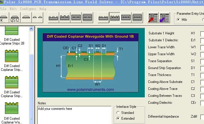
In a typical mobile phone PCB stackup, there are multiple signal layers, often placed on the outer surfaces or between ground planes to shield them from noise. Designers route traces on these layers with precision, maintaining controlled impedance (commonly 50 ohms for RF signals) to ensure signal integrity. Poor routing can lead to signal loss or delays, directly impacting the phone’s responsiveness.
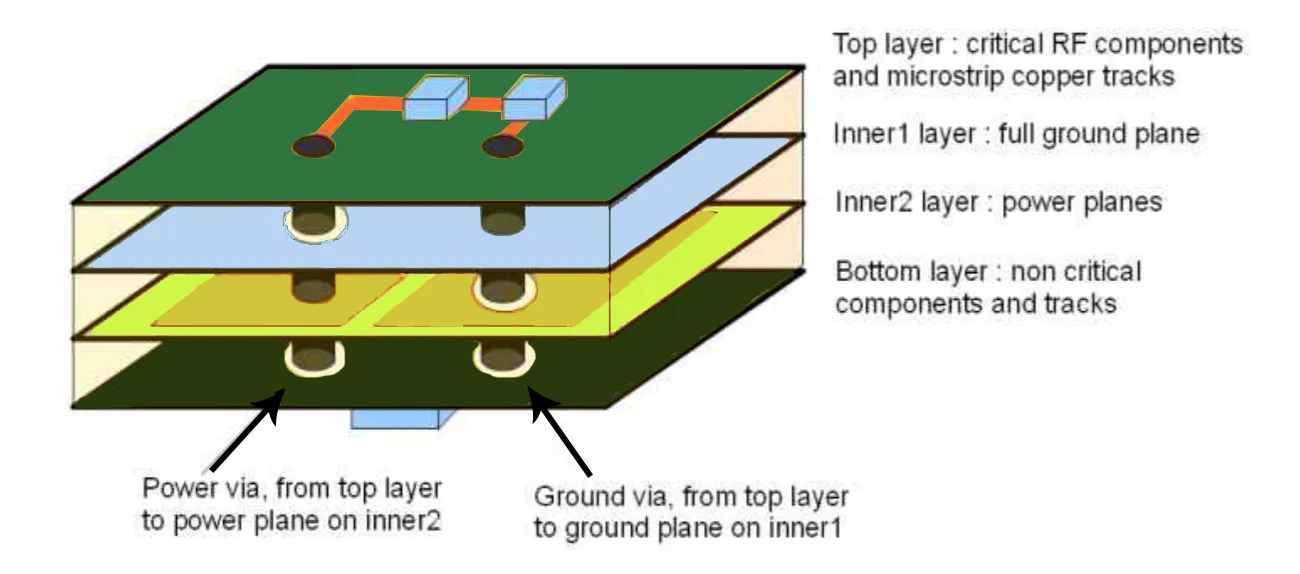
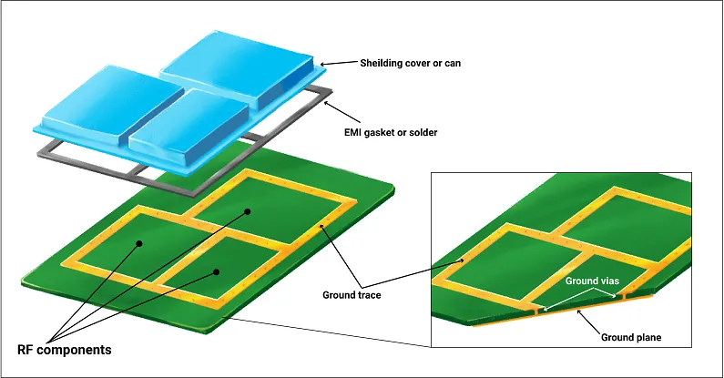
2. Ground Plane PCB: Shielding and Stability
The ground plane is a vital layer in any multilayer PCB, acting as a reference point for all signals and providing a return path for current. In mobile phones, ground planes are crucial for reducing electromagnetic interference (EMI) and ensuring stable operation of high-speed circuits.
Ground planes are often placed adjacent to signal layers to shield them from external noise and crosstalk. A solid ground plane also helps with heat dissipation, which is essential given the compact nature of mobile devices. Without a proper ground plane, a phone’s performance could suffer from random glitches or even complete failure of components.
3. Power Plane PCB: Delivering Consistent Voltage
Power planes are dedicated layers that distribute voltage to various components on the board. In a mobile phone, where different chips may require voltages ranging from 1.1V for processors to 3.8V for battery management, power planes ensure a stable and noise-free supply. This is critical for preventing performance drops or damage to sensitive components.
Power planes are usually placed in the inner layers of the PCB stackup, close to the components they serve, to minimize voltage drops. They are often paired with ground planes to form a low-impedance power distribution network, reducing noise and improving efficiency. For example, a typical mobile phone PCB might have a power plane delivering a steady 1.8V to memory chips, ensuring they operate without interruption.
Related Reading: Signal Integrity Issues in Mobile Phone PCB Layout: Causes and Solutions
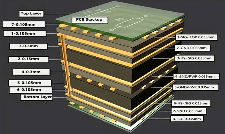
Typical PCB Layer Stackup in Mobile Phones
While the exact number of layers varies based on the phone’s features, a common configuration for mid-range to high-end devices is an 8-layer PCB stackup. Here’s an example of how these layers might be arranged:
- Top Layer (Signal Layer): Used for high-speed signals and component mounting.
- Layer 2 (Ground Plane): Shields the top signal layer and provides a return path.
- Layer 3 (Signal Layer): Routes additional signals, often for data or control.
- Layer 4 (Power Plane): Distributes voltage to components above and below.
- Layer 5 (Power Plane): Supplies a different voltage level if needed.
- Layer 6 (Signal Layer): Handles more signal routing.
- Layer 7 (Ground Plane): Shields lower signal layers and aids heat dissipation.
- Bottom Layer (Signal Layer): Used for additional components or low-speed signals.
This stackup ensures that signal layers are protected by adjacent ground planes, while power planes are centrally located for efficient distribution. The arrangement also helps manage thermal performance, as inner layers can dissipate heat more effectively.
Challenges in Designing PCB Layer Stackups for Mobile Phones
Designing a multilayer PCB for mobile phones is no easy task. Engineers face several challenges that must be addressed to ensure the device performs reliably.
1. Miniaturization
Mobile phones are getting thinner, yet they’re expected to include more features. This pushes PCB designers to use thinner layers and smaller vias (connections between layers), often as small as 0.1 mm in diameter. High-density interconnect (HDI) technology is commonly used in mobile phone PCBs to achieve this level of miniaturization, allowing for more layers in a smaller space.
2. Signal Integrity at High Frequencies
With 5G and other high-speed technologies, mobile phone PCBs must handle signals at frequencies up to 5 GHz or higher. At these speeds, even a small mismatch in impedance—say, deviating from the standard 50 ohms—can cause signal reflection and data loss. Engineers use precise trace widths and dielectric materials with low loss (like FR-4 or advanced laminates) to maintain signal quality.
3. Thermal Management
Modern mobile phones generate significant heat, especially during gaming or video streaming. Without proper layer arrangement, this heat can damage components or reduce performance. Ground and power planes often double as heat sinks, while vias are used to transfer heat to outer layers for dissipation.
Best Practices for PCB Layer Stackup Design
For engineers or designers working on mobile phone PCBs, following best practices can make a big difference in performance and reliability. Here are some key tips:
- Alternate Signal and Ground Layers: Always place ground planes next to signal layers to minimize noise and crosstalk.
- Centralize Power Planes: Position power planes in the middle of the stackup for even distribution and reduced interference.
- Use Controlled Impedance: Design signal traces with specific widths and spacing to match impedance requirements, such as 50 ohms for RF signals.
- Optimize Via Placement: Use microvias and blind vias to save space and maintain signal integrity in HDI designs.
- Choose the Right Materials: Select dielectric materials with appropriate thickness and low dielectric constant (Dk) values, typically around 3.5 to 4.5 for mobile phone PCBs, to support high-speed signals.
Related Reading: Understanding PCB Layers: A Beginner's Perspective
How PCB Layers Impact Mobile Phone Performance
The way PCB layers are arranged directly affects a mobile phone’s speed, battery life, and connectivity. For instance, poor grounding can lead to EMI, causing dropped calls or slow data speeds. Similarly, an inefficient power plane design might result in voltage drops, reducing battery efficiency or causing random shutdowns.
On the flip side, a well-designed multilayer PCB stackup ensures smooth operation. High-speed signals travel without interference, power is delivered consistently, and heat is managed effectively. This is why flagship phones with advanced features often use 10-layer or even 12-layer PCBs, compared to 6-layer designs in budget models.
Conclusion: The Backbone of Mobile Technology
The PCB layer stackup is the unsung hero of mobile phone design. By carefully arranging signal layer PCBs, ground plane PCBs, and power plane PCBs within a multilayer PCB, engineers create devices that are compact, powerful, and reliable. Understanding these layers and their roles—whether it’s shielding signals with ground planes or ensuring stable voltage with power planes—gives insight into the complexity behind the smartphones we rely on daily.
At ALLPCB, we’re passionate about supporting innovative designs with high-quality PCB manufacturing solutions. Whether you’re working on a mobile phone prototype or another cutting-edge project, mastering the art of PCB layer stackup is the first step to success. With the right approach, you can build devices that push the boundaries of technology while meeting the strict demands of modern electronics.


