 ALLPCB


Introduction
PCB drilling clearances play a vital role in ensuring the integrity and reliability of printed circuit boards during manufacturing and operation. These clearances define the spatial relationships between drilled holes and surrounding copper features, directly influencing electrical performance and structural durability. In PCB design rules, parameters such as drill-to-copper clearance and annular ring become essential to prevent defects like shorts or plating failures. Engineers must prioritize these aspects to achieve optimal manufacturability, especially in high-density designs where tolerances are tight. Understanding PCB drilling clearances helps designers balance functionality with production feasibility, reducing costly rework and enhancing overall board quality. This article explores the principles, best practices, and implications of these critical design elements.
What Are PCB Drilling Clearances?
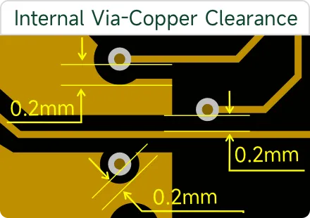
PCB drilling clearances refer to the minimum distances maintained between the edges of drilled holes and adjacent copper elements on the board. The primary components include drill-to-copper clearance, which is the space from the drill path to the nearest trace, pad, or plane, and the annular ring, defined as the copper width encircling a plated through-hole or via. Minimum spacing rules extend these concepts to ensure no unintended contacts occur during fabrication. These clearances account for mechanical tolerances in drilling equipment and material behaviors under stress. Inadequate PCB drilling clearances can lead to drill breakout, where the bit encroaches on copper, compromising conductivity. Designers incorporate these into PCB design rules to align with industry expectations for reliability.
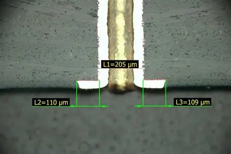
Annular rings serve as the connective bridge between holes and traces, providing tolerance for positional inaccuracies. External annular rings appear on surface layers, while internal ones exist between cores, demanding precise layer registration. Drill-to-copper clearance protects nearby features from mechanical damage or debris during the drilling process. Together, these elements form the foundation of robust hole geometries in multilayer boards. Standards like IPC-2221 outline guidelines for land proportions to support these clearances effectively.
Why PCB Drilling Clearances Matter in Design and Manufacturing
Proper PCB drilling clearances are crucial for preventing manufacturing defects that could cascade into field failures. Drill bit wander, a common issue with smaller diameters, can cause the hole to deviate from its programmed center, potentially eroding the annular ring if clearances are insufficient. This leads to reduced plating thickness or outright ring lift-off, violating acceptability criteria in IPC-A-600. Manufacturability suffers when clearances force compromises in drill selection or aspect ratios, increasing cycle times and costs. Electrical reliability also hinges on these spaces, as poor clearances risk shorts between nets post-plating.
In high-reliability applications, such as aerospace or medical devices, stringent PCB design rules mandate generous clearances to accommodate environmental stresses like thermal cycling. Plating buildup inside holes narrows the effective diameter, amplifying the importance of initial drill-to-copper clearance to avoid encroachment on traces. Minimum spacing violations often result in yield losses, as fabricators reject boards failing visual or electrical tests. By optimizing these parameters, engineers enhance signal integrity and mechanical strength across the board lifecycle. Ultimately, PCB drilling clearances bridge design intent with production reality, ensuring consistent performance.
Technical Principles Behind PCB Drilling Clearances
The mechanics of PCB drilling involve high-speed carbide bits that generate heat and vibration, influencing clearance requirements. Positional tolerances in CNC drilling machines, combined with board flexure, necessitate buffer zones around holes to prevent copper damage. Annular ring dimensions must withstand plating processes, where copper deposition occurs both inside the hole and on pad surfaces. IPC-6012 specifications address performance qualifications, including hole wall quality tied to adequate clearances. Internal layers face heightened challenges due to sequential lamination, where misalignment can thin annular rings below functional limits.
Drill-to-copper clearance directly counters plating shrinkage effects, as electrolytic copper adds thickness that shifts boundaries. Minimum spacing between multiple holes or features prevents crosstalk during drilling debris removal via plasma or chemical desmear. Aspect ratio, the board thickness to hole diameter ratio, indirectly governs clearances, as deeper holes amplify wander risks. Engineers model these interactions using design software rule checks, simulating tolerances for worst-case scenarios. These principles underscore why PCB drilling clearances form a cornerstone of defect-free fabrication.
Fabricators employ routing sequences to minimize stress on clearances, drilling larger holes first to reduce panel warp. Copper weight variations across layers affect clearance efficacy, with heavier foils demanding wider margins. Post-drill inspections verify annular ring continuity, flagging issues early. Understanding these dynamics empowers designers to specify manufacturable layouts without overdesign.
Incorporating PCB Drilling Clearances into Design Rules
Effective PCB design rules integrate drilling clearances as hard constraints checked during layout. Start by defining drill-to-copper clearance based on hole size, typically scaling with diameter to offset wander. Annular ring targets follow class-specific guidelines, ensuring external rings fully encircle holes while internal ones maintain connectivity. Minimum spacing rules extend to plane cutouts and trace routings near holes, preventing sliver defects. Tools automate these verifications, flagging violations before Gerber export.
Consider board stackup when setting clearances, as core thicknesses impact registration accuracy. For high-layer counts, increase drill-to-copper margins to buffer lamination shifts. Aspect ratio limits guide hole sizing, indirectly supporting clearances by favoring feasible drills. Collaborate with fabricators early to align rules with their capabilities, optimizing for cost and speed. Regular design reviews refine these parameters, incorporating lessons from prior builds.
- Drill-to-Copper — Key considerations: Drill diameter, plating buildup; Impact on manufacturability: Prevents shorts and debris issues.
- Annular Ring (External) — Key considerations: Pad size minus finished hole; Impact on manufacturability: Ensures via reliability.
- Annular Ring (Internal) — Key considerations: Layer alignment tolerance; Impact on manufacturability: Supports multilayer integrity.
- Minimum Hole Spacing — Key considerations: Edge-to-edge distance; Impact on manufacturability: Avoids drill interference.
This summary highlights core elements, aiding quick rule reference in design flows.
Best Practices for Optimizing PCB Drilling Clearances
Adopt conservative clearances for production prototypes to validate manufacturability before scaling. Use the largest viable drill sizes to relax clearance demands, especially in thick boards. Implement tenting or plugging for non-critical vias to protect annular rings during soldering. Simulate drill wander in design tools, adjusting pads dynamically. Prioritize sequential drilling in panel layouts to preserve clearances under mechanical loads.
Layer-specific rules enhance precision: tighter external clearances suffice due to better access, while internals require padding. Monitor copper distribution to avoid imbalance near holes, which strains clearances. Post-design DFM analysis confirms compliance, iterating as needed. These practices minimize rejects and accelerate time-to-market.
Troubleshooting Common Issues with PCB Drilling Clearances
Designers often encounter annular ring breakout in high-density boards, signaled by fab reports of nicked copper. Root causes include undersized pads or overlooked drill tolerances; remedies involve upsizing lands proportionally. Internal ring fractures appear in cross-sections, traced to lamination misalignment, fixable by tighter registration specs. Excessive drill-to-copper violations manifest as plating bridges, resolved by widening spaces pre-plating.
Debris-induced shorts near holes stem from inadequate minimum spacing, addressed via optimized desmear processes. Thermal stress testing reveals weak annular rings, prompting reinforcement with larger dimensions. Systematic audits of design rules catch these preemptively. Case studies show that standardizing clearances per IPC guidelines cuts defect rates significantly.
Conclusion
Mastering PCB drilling clearances elevates design quality, ensuring robust manufacturability and long-term reliability. Key elements like drill-to-copper clearance, annular ring, and minimum spacing interlink to safeguard against fabrication pitfalls. By embedding these into PCB design rules and adhering to standards such as IPC-2221, IPC-6012, and IPC-A-600, engineers mitigate risks effectively. Proactive best practices and troubleshooting foster iterative improvements. Prioritizing these aspects yields boards that perform consistently under demanding conditions, streamlining production workflows.
FAQs
Q1: What is drill-to-copper clearance in PCB design?
A1: Drill-to-copper clearance is the minimum distance between a drilled hole's edge and the nearest copper feature, such as traces or pads. It prevents mechanical damage during drilling and accounts for plating buildup. Proper sizing enhances manufacturability by avoiding shorts or rejects. Engineers set this in PCB design rules based on hole size and tolerances for reliable fabrication.
Q2: How does annular ring affect PCB drilling clearances?
A2: The annular ring is the copper width around a plated hole, providing tolerance for drill inaccuracies. It integrates with drill-to-copper clearance to ensure plating integrity and connectivity. Insufficient rings lead to breakout or weak joints, impacting reliability. Standards like IPC-A-600 define acceptability, guiding minimum dimensions in multilayer designs.
Q3: Why are minimum spacing rules important for PCB manufacturability?
A3: Minimum spacing rules dictate distances between holes, traces, and features near drills, preventing interference and debris issues. They support overall PCB drilling clearances by maintaining isolation during processing. Violations increase defect risks, extending lead times. Incorporating them into design rules optimizes yield and cost-effectiveness for production.
Q4: What role do industry standards play in PCB design rules for clearances?
A4: Standards like IPC-2221 and IPC-6012 provide frameworks for annular ring and clearance dimensions across reliability classes. They ensure consistency in drill-to-copper and minimum spacing, aligning design with fabrication capabilities. Adhering to these promotes manufacturability and performance verification through qualification tests.


