ALLPCB


Introduction
Aluminum printed circuit boards, often called aluminum PCBs or metal core PCBs, excel in applications demanding superior thermal management, such as power electronics, LED lighting, and automotive systems. The stackup design forms the foundation of their performance, dictating heat dissipation, electrical isolation, and mechanical stability. Engineers must optimize the aluminum PCB stackup layers to balance thermal conductivity with electrical requirements, ensuring reliable operation under high power densities. Poor stackup choices lead to hotspots, warpage, or failures, while well-designed configurations enhance longevity and efficiency. This guide delves into key elements like aluminum PCB dielectric thickness, aluminum PCB copper thickness, aluminum PCB impedance control, and aluminum PCB signal integrity. By following structured principles, electric engineers can achieve robust designs aligned with industry needs.
What Is Aluminum PCB Stackup and Why It Matters
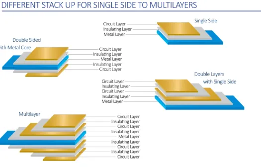
Aluminum PCB stackup refers to the precise arrangement of conductive, insulating, and substrate layers that form the board structure. Typically, it consists of a copper circuit layer bonded to a thermally conductive dielectric over an aluminum base plate. This configuration differs from standard FR4 multilayers by prioritizing heat spreading rather than interlayer routing complexity. Single-sided stackups suit simple power applications, while double-sided variants accommodate more traces on both surfaces.
The relevance stems from aluminum's high thermal conductivity, around 200 W/m·K, which rapidly conducts heat from components to heatsinks. In high-current scenarios, improper stackup causes thermal runaway, reducing component lifespan. Optimizing aluminum PCB stackup layers prevents such issues, supporting denser layouts and higher frequencies. Reliability improves as uniform heat distribution minimizes CTE mismatches between layers. For electric engineers, mastering stackup ensures compliance with performance demands in demanding environments.
Key Components of Aluminum PCB Stackup Layers
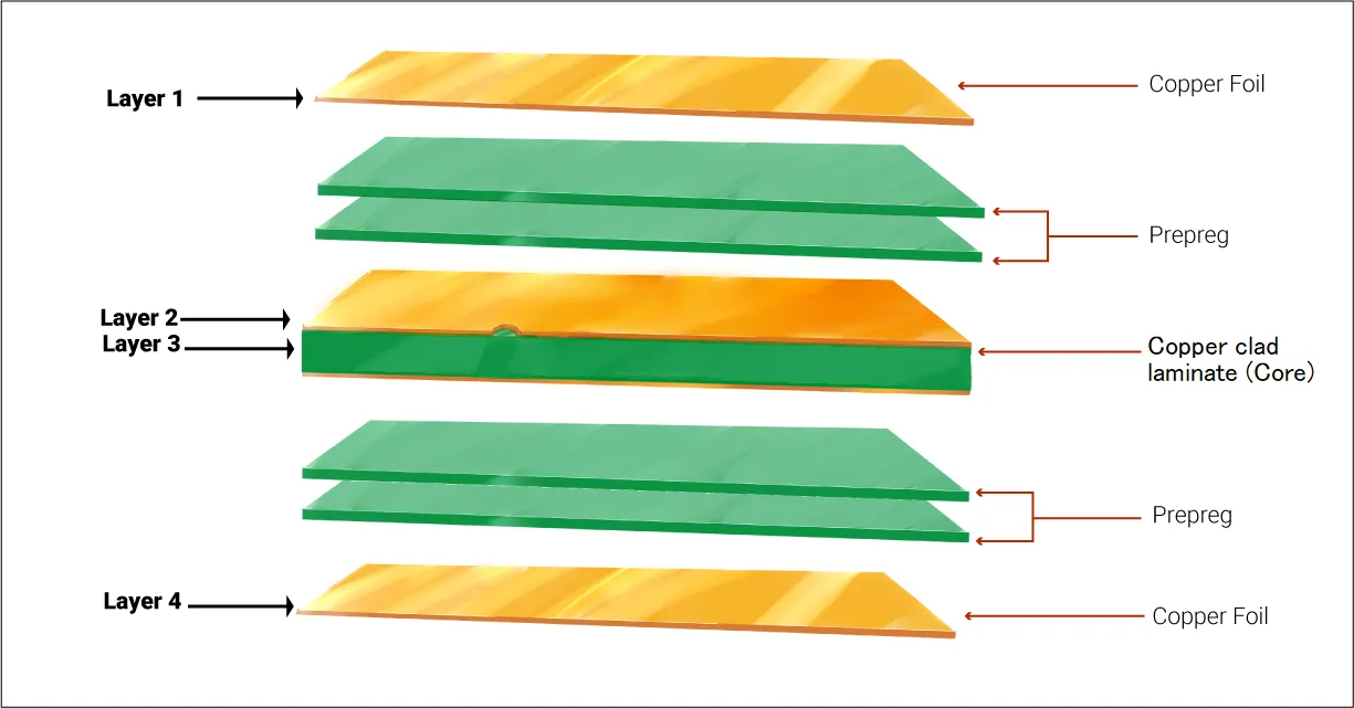
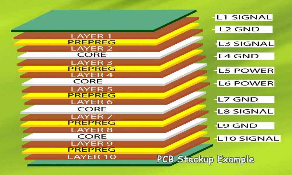
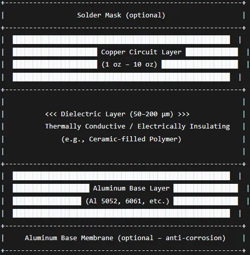
Aluminum PCB stackup layers generally include three primary elements: the top copper foil for circuits, the dielectric insulator, and the aluminum substrate. Single-layer designs feature one copper layer directly over the dielectric, ideal for mounting high-power devices like LEDs or MOSFETs. Double-layer stackups add a second copper layer separated by additional dielectric, enabling ground planes or signal routing on the underside. Though rare, hybrid configurations incorporate FR4 cores for multilayer signal routing atop the metal base, but these demand careful thermal isolation.
Layer sequencing affects overall board rigidity and expansion. The aluminum base, typically dominating thickness, anchors the stackup and serves as a heat sink interface. Circuit layers handle current and signals, while dielectrics provide electrical isolation without impeding heat flow. Engineers select layer counts based on trace density and thermal loads, often simulating via finite element analysis. Adhering to design guidelines like those in IPC-2221 ensures layer interfaces withstand mechanical stresses.
Optimizing Aluminum PCB Dielectric Thickness
Aluminum PCB dielectric thickness critically influences thermal resistance and voltage breakdown strength. Common materials, ceramic-filled epoxies or polyimides, offer thermal conductivities from 1 to 8 W/m·K, with thicknesses ranging from 75 to 150 microns in standard applications. Thinner dielectrics reduce thermal impedance, accelerating heat transfer to the aluminum base, but risk dielectric puncture under high voltages. Conversely, thicker layers enhance isolation for high-voltage designs, though at the cost of elevated junction temperatures.
Selection involves trade-offs: for 1000V applications, 150-micron dielectrics provide ample margin, while 100-micron suits lower voltages with better cooling. Thermal resistance scales inversely with thickness, following Fourier's law, so simulations predict hotspot risks. Fabricators control thickness uniformity to avoid weak points. Engineers verify designs against voltage ratings, ensuring dielectric withstand exceeds operational peaks by 20-50%. Consistent thickness also aids warpage control during reflow.
Related Reading: How to Choose the Best Dielectric Material for Aluminum PCBs
Selecting Aluminum PCB Copper Thickness
Aluminum PCB copper thickness determines current-carrying capacity and trace resistance. Standard foils range from 1 oz/ft2 (35 μm) for fine-pitch signals to 3-5 oz/ft2 (105-175 μm) for heavy power traces, with heavy copper up to 10 oz for extreme currents. Thicker copper lowers I2R losses and supports wider traces, but increases etching challenges and board weight. In power designs, 2 oz copper balances thermal mass with manufacturability, aiding transient heat absorption.
Per IPC-2221 current-carrying guidelines, trace width scales with thickness and allowable temperature rise. For example, a 2 oz trace at 30°C rise carries more ampacity than 1 oz equivalents. Copper also contributes to overall thermal spreading before heat reaches the dielectric. Engineers model Joule heating in stackups to prevent hotspots. Surface treatments like HASL or ENIG protect thicker foils from oxidation.
Related Reading: Complete Guide to Aluminum PCB
Aluminum PCB Impedance Control Strategies
Aluminum PCB impedance control manages transmission line characteristics despite the thin dielectric and metal base. Characteristic impedance Z0 depends on trace width, dielectric constant (Dk around 4-5), and height above the aluminum plane. For 50Ω microstrips, wider traces compensate for proximity to the low-impedance base, often requiring 10-20 mil widths. Controlled impedance becomes essential in RF power amplifiers or mixed-signal boards where aluminum aids cooling.
Calculations use equations like Z0 = (87 / √(Dk+1.41)) * ln(5.98h / (0.8w + t)), adapted for metal-backed substrates. Fabricators test coupons post-lamination to verify ±10% tolerance. Ground vias and stitching minimize return path inductance. Unlike FR4, the aluminum plane acts as a natural reference, but CTE differences demand via relief. Simulations with field solvers optimize for minimal reflections.
Ensuring Aluminum PCB Signal Integrity
Aluminum PCB signal integrity hinges on controlling reflections, crosstalk, and losses in high-frequency paths. The solid aluminum base reduces EMI by shielding, but thin dielectrics heighten capacitance, lowering cutoff frequencies. Signal distortion arises from impedance discontinuities at vias or bends, exacerbated by thermal expansion mismatches. Engineers employ length-matched routing and serpentine patterns for differential pairs.
Thermal vias enhance integrity by equalizing temperatures, preventing Dk variations that shift delays. Eye diagram analysis reveals jitter from ground bounce. Pre-emphasis drivers compensate dielectric absorption. Stackup symmetry, even in single-sided boards, aids return currents. Testing per high-speed protocols confirms bit error rates below 10^-12.
Best Practices for Aluminum PCB Stackup Design
Start with thermal modeling to predict junction-to-ambient resistance. Prioritize direct component-to-aluminum paths via thermal pads and vias filled with conductive epoxy. Balance copper pours for uniform CTE, minimizing warpage per IPC-6012 performance specs. Specify dielectric thickness conservatively for voltage, and simulate impedance early.
Incorporate blind vias to avoid base penetration, preserving heat flow. Use symmetric stackups for double-sided to equalize stresses. Prototype with varied copper weights to validate current ratings. Collaborate with fabricators on panelization for warpage control. Final DFM checks ensure annular rings and clearances meet class 3 requirements.
Conclusion
Effective aluminum PCB stackup design integrates aluminum PCB stackup layers, dielectric and copper thicknesses, impedance control, and signal integrity for peak performance. Logical optimization yields reliable boards that excel in thermal-heavy applications. Engineers benefit from structured simulations and standard adherence, avoiding common pitfalls like hotspots or distortions. Implementing these principles elevates design quality, extending system reliability.
FAQs
Q1: What are the typical aluminum PCB stackup layers for high-power LED applications?
A1: Aluminum PCB stackup layers usually comprise a 1-2 oz copper circuit layer, 100-150 micron dielectric, and 1.5 mm aluminum base. This setup ensures low thermal resistance while supporting high currents. Single-layer configurations dominate for simplicity, with thermal vias linking components to the base. Double-sided adds underside grounding for better EMI control. Always simulate heat flow to confirm layer efficacy.
Q2: How does aluminum PCB dielectric thickness affect thermal performance?
A2: Aluminum PCB dielectric thickness directly impacts thermal resistance; thinner layers like 75-100 microns lower impedance to heat flow, ideal for high-density power. Thicker options up to 200 microns boost voltage isolation but raise temperatures. Select based on power dissipation and breakdown needs, verifying via models. Uniformity prevents hotspots.
Q3: Why is aluminum PCB copper thickness critical for impedance control?
A3: Aluminum PCB copper thickness influences skin effect and trace impedance at high frequencies. Thicker foils (2-3 oz) widen traces for 50Ω control over thin dielectrics. They also enhance current capacity without excessive resistance. Model with field solvers for tolerance.
Q4: How to maintain aluminum PCB signal integrity in mixed-signal designs?
A4: Aluminum PCB signal integrity relies on impedance-matched traces, ground stitching, and thermal vias to stabilize Dk. Minimize via stubs and use reference planes. Simulate TDR for reflections. The metal base aids shielding but requires careful routing.
References
IPC-2221B — Generic Standard on Printed Board Design. IPC, 2012
IPC-6012E — Qualification and Performance Specification for Rigid Printed Boards. IPC, 2017
IPC-A-600K — Acceptability of Printed Boards. IPC, 2020