 ALLPCB


Printed circuit boards form the foundation of nearly every electronic device used in industrial, automotive, and consumer applications. Engineers responsible for system performance recognize that even minor defects introduced during fabrication or assembly can lead to field failures, costly recalls, and compromised safety. Systematic inspection therefore serves as a critical checkpoint that directly influences overall product reliability. By identifying deviations early, teams can maintain consistent electrical performance and mechanical integrity across production batches. This approach supports long-term operational stability without relying on post-delivery corrections.
Why PCB Inspection Matters for Reliability
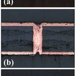
Product reliability depends on the ability of a PCB to withstand thermal cycling, mechanical stress, and environmental exposure over its intended lifespan. Inspection processes allow engineers to verify that copper traces maintain correct geometry, vias exhibit proper plating thickness, and solder joints achieve adequate wetting. When these parameters fall outside acceptable limits, the risk of intermittent connections or complete circuit failure increases significantly. Comprehensive inspection therefore reduces the incidence of PCB failure analysis investigations after deployment. It also strengthens PCB quality assurance programs by providing measurable data at each manufacturing stage. Engineers can then correlate inspection results with predicted service life, enabling more accurate design margins.
Technical Principles of PCB Inspection
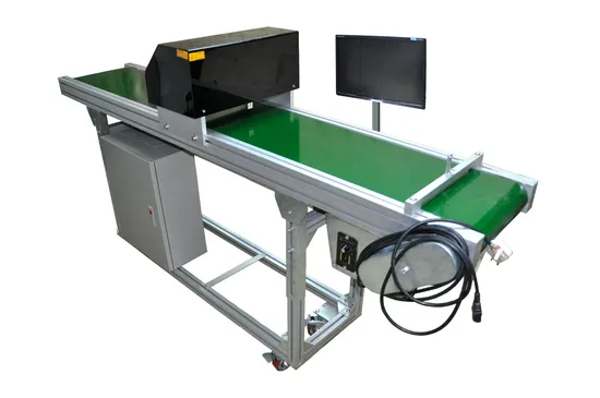
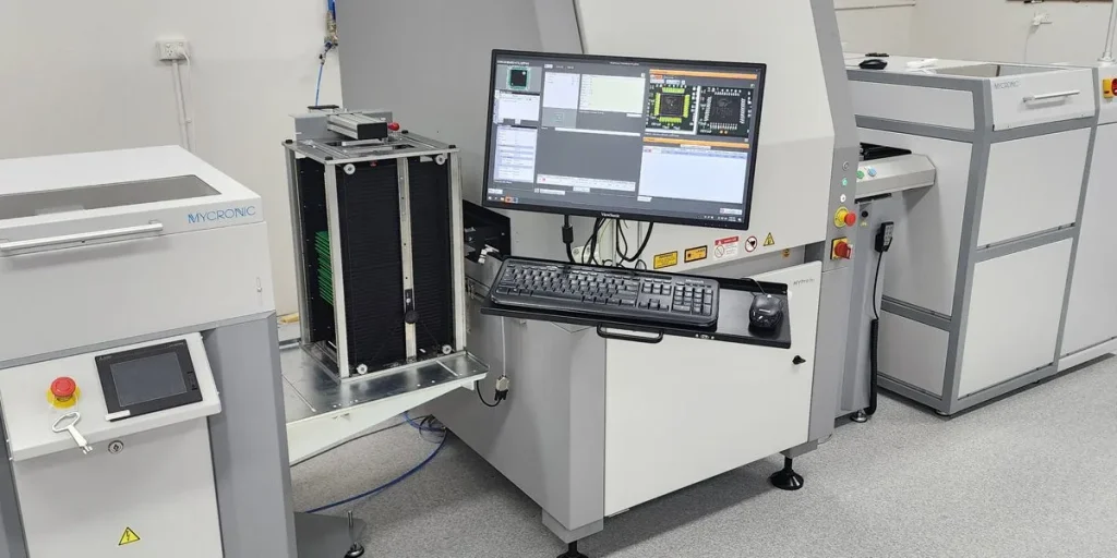
Inspection begins with visual examination to detect surface anomalies such as scratches, contamination, or misaligned components. Automated optical inspection systems extend this capability by comparing captured images against reference designs, flagging discrepancies in trace width or spacing. X-ray imaging then reveals hidden features including voids in solder joints and internal layer registration errors that optical methods cannot observe. Electrical testing follows to confirm continuity and isolation between nets, ensuring no open circuits or unintended shorts exist. These layered techniques together address both visible and latent defects that affect PCB reliability.
Thermal and mechanical stresses during operation can exacerbate small manufacturing variations into functional failures. Warpage measurement, for example, quantifies board flatness after reflow, because excessive distortion may fracture solder joints or damage components. Delamination testing evaluates adhesion between laminate layers under elevated temperature and humidity conditions. By applying these principles consistently, engineers obtain quantitative indicators of long-term durability rather than relying solely on visual acceptance.
Related Reading: The Beginner's Guide to Visual PCB Inspection: Identifying Common Defects
PCB Testing Standards and Quality Assurance
Industry standards provide the acceptance criteria that transform raw inspection data into actionable decisions. Criteria defined in IPC-A-600 guide the evaluation of external and internal board features, specifying allowable limits for voids, cracks, and plating irregularities. When combined with electrical verification protocols, these standards help maintain uniform PCB quality assurance across multiple suppliers and production runs. Engineers reference the same criteria during incoming inspection and final audit, creating a traceable record that supports root-cause investigations if field issues arise.
Best Practices in PCB Inspection
Effective programs integrate inspection at multiple points rather than concentrating all checks at the end of the line. Incoming material verification confirms laminate quality and copper foil consistency before processing begins. In-process monitoring after etching and drilling catches dimensional errors before they propagate into subsequent operations. Post-assembly inspection, including both optical and X-ray methods, validates solder joint integrity and component placement accuracy. Documentation of each inspection stage allows engineers to track trends and adjust process parameters proactively.
Sampling plans should reflect the criticality of the application. High-reliability sectors such as aerospace or medical devices typically employ 100 percent inspection for key attributes, while less demanding products may use statistical sampling. Calibration of inspection equipment remains essential to ensure measurement repeatability and reproducibility. Regular correlation between different inspection methods further reduces false positives and missed defects, preserving confidence in the overall PCB reliability assessment.
Related Reading: The Ultimate Guide to PCB Inspection: Techniques and Technologies
Conclusion
PCB inspection functions as an engineering control that directly supports product reliability by catching defects before they reach the customer. Structured application of visual, automated, and electrical methods, guided by recognized industry criteria, enables consistent quality outcomes. Engineers who embed these practices into their development and manufacturing workflows achieve lower failure rates and more predictable field performance. The result is reduced PCB failure analysis workload and stronger overall PCB quality assurance.
FAQs
Q1: How does PCB inspection contribute to PCB reliability?
A1: Systematic inspection identifies dimensional, plating, and assembly defects before they cause electrical or mechanical failures in service. By verifying compliance with defined acceptance limits at each stage, engineers can prevent latent issues from progressing into field returns. This proactive approach reduces the frequency of PCB failure analysis and supports predictable long-term operation across temperature and vibration environments.
Q2: What role do PCB testing standards play in quality assurance?
A2: Standards establish uniform acceptance criteria for features such as trace geometry, via fill, and solder joint appearance. When applied consistently during incoming, in-process, and final inspection, they create measurable benchmarks that align design intent with manufacturing output. Engineers use these criteria to document compliance and facilitate traceability when investigating any deviation from expected PCB reliability performance.
Q3: Why is early detection of warpage important for PCB reliability?
A3: Excessive warpage after thermal excursions can induce stress on solder joints and component leads, leading to cracks or intermittent connections over time. Measurement during inspection allows process adjustments before boards proceed to final assembly. Early correction therefore minimizes the risk of premature failure and reduces the need for subsequent PCB failure analysis in deployed systems.
Q4: How can engineers improve PCB quality assurance through inspection?
A4: Engineers strengthen quality assurance by placing inspection points after critical operations and correlating results with design specifications. Combining optical, X-ray, and electrical methods provides comprehensive coverage of both surface and internal features. Documented trends from these checks enable continuous process refinement and sustained improvement in overall PCB reliability.





