ALLPCB


The Role of High-Layer-Count PCBs in 5G Infrastructure
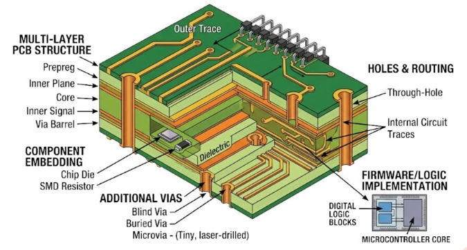
High-layer-count PCBs form a critical foundation for 5G infrastructure by enabling the dense interconnects and signal integrity required in base stations, core network equipment, and massive MIMO antennas. These boards typically exceed 20 layers and support the high data rates, low latency, and complex routing demands of fifth-generation wireless systems. Electric engineers designing 5G hardware rely on such PCBs to integrate RF front-ends, digital processors, and power distribution networks within compact form factors. The shift from 4G to 5G has increased layer counts because millimeter-wave frequencies and beamforming arrays demand additional ground planes, power planes, and controlled-impedance traces. Without sufficient layers, signal crosstalk and power noise would compromise system performance in telecommunications networks.
Why High-Layer-Count PCBs Matter for 5G Infrastructure
5G networks operate across sub-6 GHz and millimeter-wave bands, requiring PCBs that maintain signal integrity over high frequencies while managing thermal loads from power amplifiers. High-layer-count designs provide the vertical interconnect density needed for routing thousands of high-speed differential pairs and control signals between multiple chipsets. This capability directly supports the massive parallel processing in 5G baseband units and radio units. Engineers select these PCBs because they allow separation of analog RF sections from digital logic through dedicated planes, reducing electromagnetic interference. The result is reliable operation in outdoor cabinets and indoor small cells exposed to varying environmental conditions.
Technical Principles of High-Layer-Count PCB Design for 5G
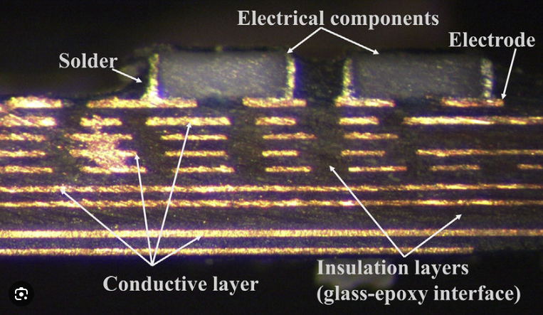
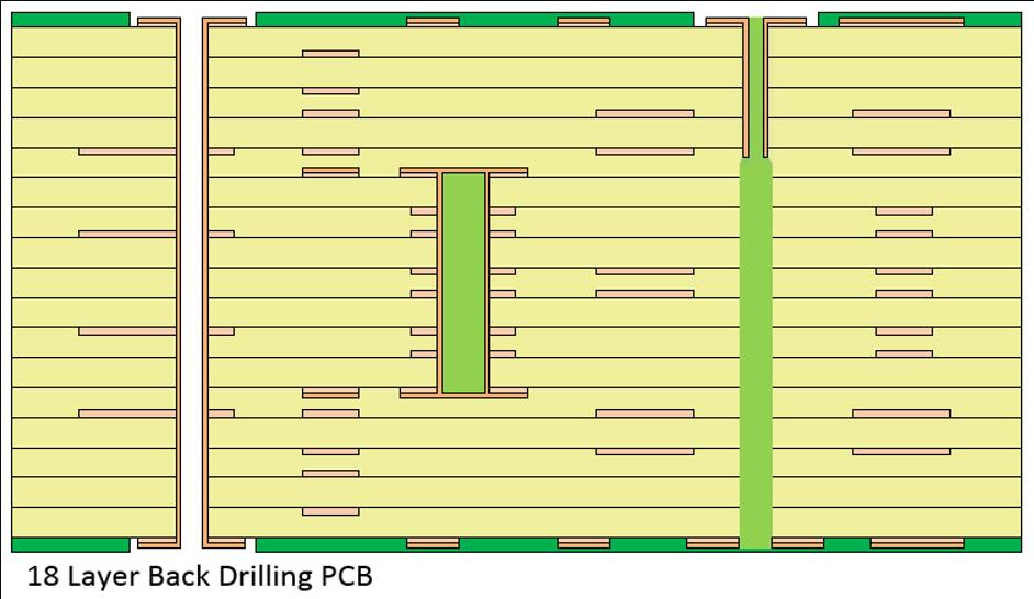
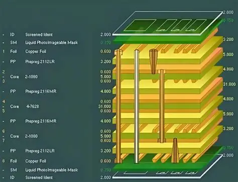
Signal integrity in high-layer-count PCBs depends on precise control of trace impedance, via stub minimization, and return-path continuity across multiple planes. Engineers use back-drilling or blind/buried vias to shorten stubs that would otherwise cause reflections at 5G frequencies. Power distribution networks incorporate multiple copper planes to achieve low inductance paths, which is essential for supplying clean power to high-current RF components. Dielectric materials must exhibit low dissipation factors to minimize insertion loss in high-frequency PCB design applications. Thermal management integrates copper pours and thermal vias that conduct heat away from hotspots toward heatsinks or chassis.
Manufacturing these boards follows strict qualification requirements outlined in IPC-6012E for rigid printed boards to ensure consistent layer registration and via reliability. High-frequency PCB design also demands careful stack-up planning so that adjacent signal layers reference solid planes, thereby containing electromagnetic fields. Engineers model the entire structure with 3D electromagnetic simulation tools to predict crosstalk and resonance before fabrication.
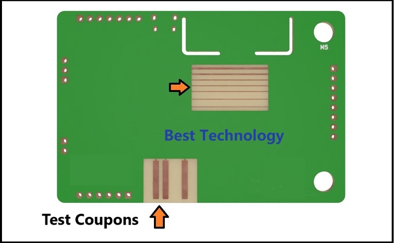
Best Practices for High-Layer-Count PCBs in Telecommunications Equipment
Design teams begin with a detailed stack-up that balances signal, power, and ground layers while maintaining overall board thickness within mechanical limits. Sequential lamination processes build the board in stages, allowing finer features on inner layers that support dense 5G routing. Controlled impedance calculations account for the dielectric constant and copper roughness at target frequencies. During layout, differential pair routing maintains consistent spacing and avoids 90-degree bends that introduce discontinuities.
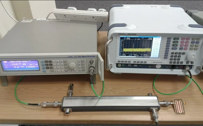
Quality control follows IPC-A-600K guidelines for acceptability of printed boards, with emphasis on annular ring, plating thickness, and void-free vias. Assembly processes prioritize low-void soldering for large BGAs and careful handling to prevent warpage in thick, multi-layer constructions. Engineers verify performance through time-domain reflectometry and vector network analyzer measurements on prototypes.
Challenges and Mitigation Strategies in 5G PCB Implementation
Warpage becomes pronounced in high-layer-count PCBs due to asymmetric copper distribution and coefficient-of-thermal-expansion mismatches between materials. Mitigation involves symmetric stack-ups and optimized cure profiles during lamination. Via reliability under thermal cycling requires attention to aspect ratios and plating quality, especially in boards exceeding 3 mm thickness. Signal loss at millimeter-wave frequencies necessitates low-loss laminates and smooth copper foils, increasing material selection complexity.
Power integrity challenges arise from simultaneous switching noise in dense digital sections; solutions include distributed decoupling capacitors and embedded capacitance layers. Engineers address these issues through iterative simulation and prototype testing rather than relying on rules of thumb alone.
Conclusion
High-layer-count PCBs enable the performance targets of 5G infrastructure by providing the necessary routing density, signal integrity, and power delivery in a single assembly. Their design and fabrication demand disciplined application of engineering principles and adherence to established qualification standards. As 5G deployments expand into higher frequency bands and denser small-cell networks, the role of these boards will continue to grow in importance for telecommunications hardware.
FAQs
Q1: What defines a high-layer-count PCB in 5G applications?
A1: A high-layer-count PCB for 5G typically contains 20 or more layers that integrate RF, digital, and power functions while maintaining controlled impedance and low loss. These boards support the complex interconnect requirements of base stations and massive MIMO systems.
Q2: How does high-layer-count PCB design improve signal integrity in 5G infrastructure?
A2: Additional layers allow dedicated reference planes and shorter via stubs, which reduce reflections and crosstalk at millimeter-wave frequencies. This approach helps engineers meet the stringent bit-error-rate targets of high-speed 5G data links.
Q3: Why are industry standards important when specifying high-layer-count PCBs for telecommunications?
A3: Standards such as IPC-6012E establish qualification criteria for layer registration, via quality, and material performance that directly affect long-term reliability in outdoor 5G equipment. Consistent application of these requirements reduces field failures.
Q4: What manufacturing considerations apply to high-layer-count PCBs used in 5G base stations?
A4: Sequential lamination, precise registration, and warpage control become critical as layer counts rise. Manufacturers must also verify plating integrity and dielectric properties to support high-frequency PCB design specifications.
References
IPC-6012E — Qualification and Performance Specification for Rigid Printed Boards. IPC, 2017
IPC-A-600K — Acceptability of Printed Boards. IPC, 2020
JEDEC J-STD-020E — Moisture/Reflow Sensitivity Classification. JEDEC, 2014