ALLPCB


Introduction
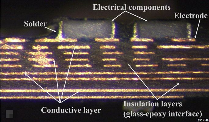
Ground planes serve as foundational elements in multilayer printed circuit board layouts. In 10-layer PCB designs, they provide essential return paths for high-speed signals while contributing to overall electromagnetic compatibility. Proper implementation of these planes helps minimize radiated and conducted emissions that can interfere with sensitive circuitry. Engineers rely on structured layer arrangements to balance signal integrity, power distribution, and thermal performance. This approach supports reliable operation in complex electronic systems where multiple signal layers coexist with power and reference planes.
Why Ground Planes Matter in 10-Layer PCB Designs
A ground plane consists of a continuous copper layer connected to the circuit reference potential. In 10-layer stackups, dedicating one or more layers to ground planes reduces the inductance of return paths compared to routed traces alone. This configuration proves especially relevant for applications involving high-frequency digital signals or mixed-signal environments. Effective 10-layer PCB ground plane design directly influences the board ability to meet performance targets without excessive noise coupling. Industry professionals recognize that inadequate plane implementation can lead to increased susceptibility to external fields and internal crosstalk.
Technical Principles of Ground Plane Design for EMI Reduction
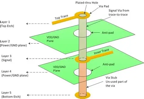
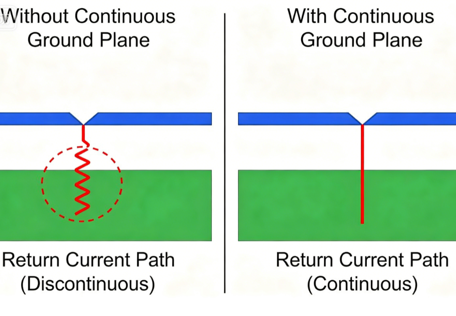
Ground planes function by offering low-impedance paths that complete current loops for signals transitioning between layers. When a signal trace routes adjacent to a solid ground plane, the return current flows directly beneath the trace, confining the electromagnetic fields and limiting radiation. In 10-layer arrangements, placing ground planes next to high-speed signal layers creates controlled impedance environments that further aid 10-layer PCB EMI reduction. Split planes or excessive voids disrupt these paths and can form unintended 10-layer PCB ground loops that act as antennas for emissions. Stitching vias connect multiple ground planes at regular intervals, maintaining equipotential surfaces across the board thickness and suppressing cavity resonances.
Signal return currents follow the path of least inductance, which a continuous plane provides more effectively than discrete traces. Capacitive coupling between adjacent layers also benefits from the shielding effect of intervening ground planes, attenuating high-frequency noise propagation. In designs with dense component placement, these mechanisms collectively lower the overall radiated emissions profile. Proper plane continuity avoids the formation of slots that could resonate at frequencies of interest in the system.
Best Practices for 10-Layer PCB Ground Plane Design
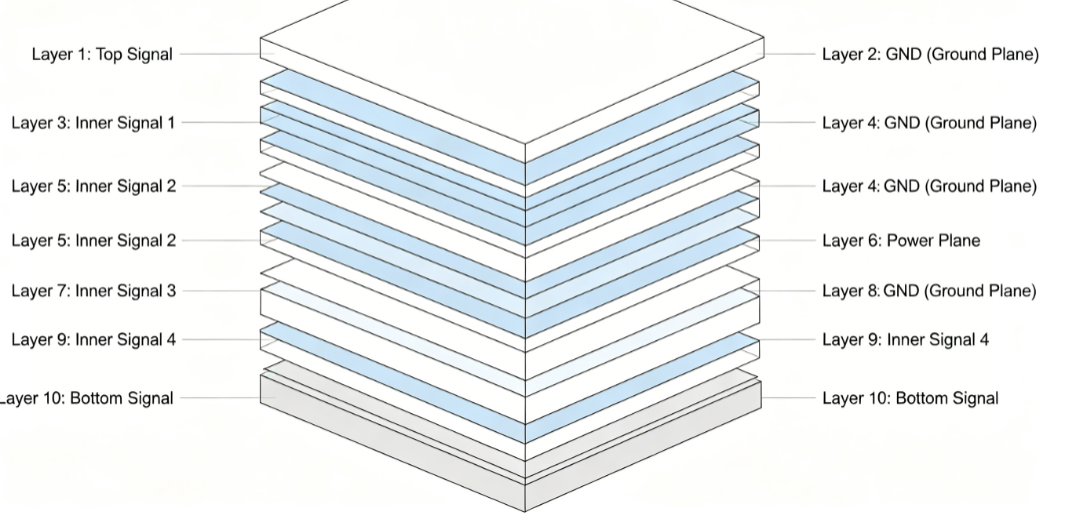
Designers begin by defining a balanced stackup that allocates sufficient layers to ground planes while accommodating signal and power requirements. Solid, unbroken ground planes on inner layers adjacent to critical signals represent a core recommendation for 10-layer PCB ground plane design. When power planes are necessary, they should pair closely with ground planes to form low-inductance capacitor structures that support decoupling. Via stitching at intervals of approximately 10 to 15 millimeters along board edges and around high-current zones maintains plane connectivity without introducing excessive thermal stress during fabrication.
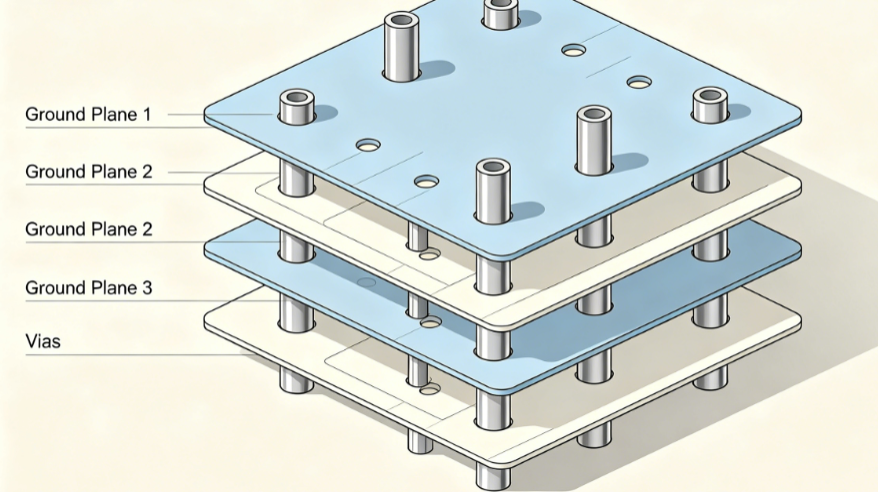
Avoiding unnecessary cuts or splits in ground planes prevents the creation of 10-layer PCB ground loops that increase loop area and associated magnetic field radiation. When isolation between analog and digital sections becomes necessary, a single-point connection strategy minimizes the risk of circulating currents. Decoupling capacitors placed near active devices benefit from short, direct connections to the nearest ground plane, reducing parasitic inductance in the power delivery network. These practices align with guidance in IPC-2221C for establishing reliable interconnect structures in multilayer boards.
Considerations for EMI Optimization in Complex 10-Layer Designs
In boards carrying mixed high-speed and low-frequency signals, careful layer assignment ensures that sensitive traces remain shielded by ground planes on both sides where possible. Thermal management integrates with ground plane usage because continuous copper areas also assist heat spreading from components. When board flexure or mechanical constraints arise, maintaining plane integrity through appropriate material selection and thickness helps preserve electrical performance. Testing for compliance often involves evaluating emissions under operational conditions to verify that the implemented 10-layer PCB EMI reduction measures achieve the desired margins.
Conclusion
Ground planes remain indispensable for achieving low EMI in 10-layer PCB designs through their roles in return path management and field containment. Structured stackup planning combined with continuous plane implementation and strategic via placement yields measurable improvements in electromagnetic compatibility. Engineers who apply these principles consistently produce boards that support higher operating frequencies with reduced noise. Attention to avoiding ground loops and maintaining plane continuity further enhances overall system reliability. These elements together form the basis for robust 10-layer PCB ground plane design practices.
FAQs
Q1: How does 10-layer PCB ground plane design contribute to EMI reduction?
A1: Continuous ground planes in a 10-layer stackup provide low-inductance return paths for signals, confining electromagnetic fields and minimizing radiation. This configuration reduces both conducted and radiated emissions when planes are placed adjacent to high-speed layers. Proper implementation also supports controlled impedance routing essential for signal integrity.
Q2: What causes 10-layer PCB ground loops and how are they avoided?
A2: Ground loops form when return currents take multiple paths due to plane discontinuities or improper connections, creating larger effective loop areas that radiate noise. Avoidance involves maintaining solid planes with minimal splits and using single-point connections where isolation is required. Regular via stitching further ensures equipotential conditions across planes.
Q3: Why prioritize ground planes in 10-layer PCB EMI reduction strategies?
A3: Ground planes offer shielding between layers and low-impedance paths that outperform discrete traces for high-frequency currents. In 10-layer designs, they enable tighter field containment and better power integrity when paired appropriately with signal layers. This approach aligns with established design standards for multilayer boards.
Q4: What role do stitching vias play in 10-layer PCB ground plane design?
A4: Stitching vias electrically connect multiple ground planes, preserving continuity and suppressing resonant modes within the board structure. They are placed at regular intervals to maintain low-impedance paths and reduce the risk of slot antennas forming at plane edges. This technique supports overall EMI performance without compromising manufacturability.
References
IPC-2221C — Generic Standard on Printed Board Design. IPC, 2023
IPC-6012E — Qualification and Performance Specification for Rigid Printed Boards. IPC, 2017