 ALLPCB


Solder mask and silkscreen layers play essential roles in printed circuit board production. These layers protect copper traces and provide component identification markings. Their selection directly influences material usage, processing steps, and overall manufacturing expenses. Engineers and procurement teams evaluate these options early in design to balance performance requirements with budget constraints. Standard choices often reduce complexity while meeting functional needs.
What Is Solder Mask and Silkscreen and Why It Matters
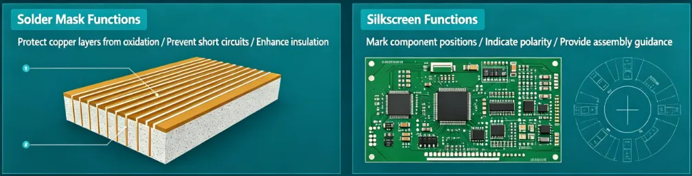
Solder mask is a polymer coating applied over copper circuitry to insulate traces and prevent solder bridging during assembly. Silkscreen, also called legend or marking, consists of ink patterns that label components, polarity indicators, and test points. Both layers add distinct steps to the fabrication sequence. Their costs arise from materials, application equipment, curing processes, and quality verification. In high-volume production, even small variations in mask thickness or ink coverage can shift total expenses noticeably. Industry standards guide acceptable quality levels for these features without mandating premium options.
Technical Principles and Mechanisms
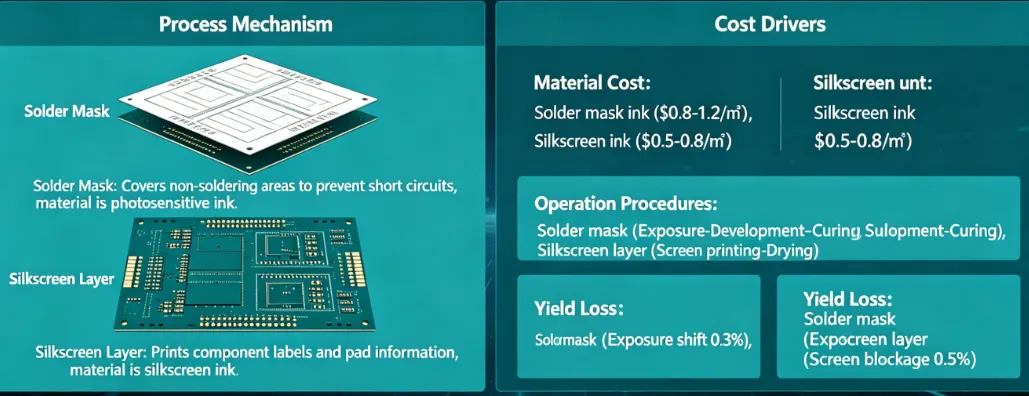
Solder mask application typically involves liquid photoimageable materials that require precise coating, exposure, development, and thermal curing. Thicker coatings or nonstandard colors increase material consumption and extend processing time. Double-sided coverage adds handling steps and inspection requirements. Silkscreen printing uses epoxy or UV-curable inks applied through screens or direct imaging systems. Higher resolution markings or additional colors demand finer screens and multiple passes, raising labor and setup costs. Yield losses from misalignment or incomplete coverage further contribute to expense. These mechanisms follow established qualification procedures outlined in IPC-6012E.
Variations in surface finish compatibility also affect outcomes. Certain mask formulations interact differently with immersion silver or electroless nickel immersion gold finishes, potentially requiring adjusted curing profiles. Silkscreen adhesion depends on surface cleanliness after mask application. Poor adhesion leads to rework or scrap, elevating per-unit costs. Manufacturing options such as matte versus glossy finishes or selective versus full coverage influence both appearance and process duration. Engineers assess these factors against electrical and environmental demands to avoid unnecessary premiums.
Practical Solutions and Best Practices
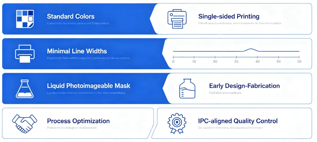
Designers achieve cost control by specifying standard green solder mask and white silkscreen unless color coding is required for assembly or identification. Limiting silkscreen to one side reduces printing cycles. Using minimum line widths and avoiding dense text clusters simplifies imaging. Selecting liquid photoimageable mask over dry film options often lowers material costs for most board thicknesses. Early collaboration between design and fabrication teams identifies opportunities to consolidate markings or eliminate redundant labels.
Process optimization includes verifying mask registration tolerances during layout review. Consistent panelization strategies allow efficient batch processing of multiple designs. Quality control checkpoints aligned with IPC-A-600K acceptance criteria help maintain yields without excessive inspection overhead. When higher contrast markings are needed, single-color high-opacity inks provide sufficient readability at lower expense than multi-color approaches. These choices preserve functionality while minimizing added steps in the production flow.
Insight into Cost Trade-offs
Common scenarios illustrate how choices accumulate. Boards requiring full solder mask on both sides incur roughly proportional increases in coating and curing time compared with single-sided coverage. Adding silkscreen on the secondary side introduces an extra alignment and curing operation. Nonstandard mask colors frequently require dedicated material batches and extended lead times. In contrast, standard options integrate seamlessly into existing production lines. Engineers review these trade-offs against assembly yield improvements that sometimes offset modest fabrication premiums.
Conclusion
Solder mask and silkscreen selections represent controllable variables in PCB manufacturing cost structures. Thoughtful specification of standard materials, coverage areas, and colors reduces processing complexity and material consumption. Adherence to recognized industry standards supports consistent quality without defaulting to premium configurations. Early evaluation during the design phase enables procurement teams to align options with volume and performance targets. The cumulative effect of these decisions supports competitive manufacturing economics across diverse applications.
FAQs
Q1: How does solder mask color affect PCB solder mask cost?
A1: Standard green solder mask remains the most economical choice because it aligns with common production setups and material availability. Nonstandard colors require separate material batches and additional process validation, increasing both direct costs and lead time. Engineers specify alternative colors only when assembly or identification needs justify the premium.
Q2: What factors influence PCB silkscreen cost during manufacturing?
A2: Silkscreen cost depends on the number of sides printed, ink color count, and marking density. Single-sided white legend on standard mask keeps processing simple. Additional colors or double-sided application add alignment steps and curing cycles. Design teams minimize text volume and line widths to control these expenses.
Q3: Can PCB legend cost be reduced without affecting assembly quality?
A3: Yes, limiting legend to essential reference designators and polarity marks reduces ink usage and imaging time. High-contrast white ink on green mask provides adequate readability for most applications. Avoiding decorative elements or redundant markings preserves identification functions at lower cost.
Q4: How do PCB manufacturing options for mask and marking impact overall project budgets?
A4: Options such as selective mask coverage or single-color legend reduce material and labor inputs compared with full-coverage or multi-color approaches. These choices integrate into standard process flows and support higher yields. Procurement teams review requirements against IPC standards to select configurations that meet performance needs efficiently.
References
IPC-6012E — Qualification and Performance Specification for Rigid Printed Boards. IPC, 2017
IPC-A-600K — Acceptability of Printed Boards. IPC, 2020
JEDEC J-STD-020E — Moisture/Reflow Sensitivity Classification. JEDEC, 2014





