 ALLPCB


Introduction
Sequential build-up PCBs represent a cornerstone in modern high-density interconnect technology, enabling compact designs for advanced electronics. These boards are constructed by sequentially adding dielectric and copper layers around a core, which demands precise material choices to ensure optimal performance. Material selection directly influences electrical integrity, signal propagation, and mechanical reliability under operational stresses. For electrical engineers working on high-speed applications, understanding how sequential build-up PCB materials affect key parameters like dielectric constant and loss tangent is essential. Thermal properties further play a critical role in preventing failures during manufacturing and use. This article explores these impacts, drawing on factory-driven insights aligned with industry standards.
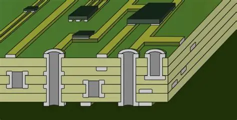
What Are Sequential Build-Up PCBs and Why Do Materials Matter?
Sequential build-up, often abbreviated as SBU, involves iterative lamination processes to create fine-line features and microvias in high-density interconnect boards. Unlike traditional multilayer PCBs, SBU starts with a core substrate and builds outer layers sequentially, allowing for tighter pitches and higher layer counts. This method is prevalent in applications requiring superior routing density, such as smartphones, automotive electronics, and data centers. However, the performance of sequential build-up PCBs hinges on the dielectric materials used between copper layers, as they dictate signal speed and attenuation. Poor material choices can lead to impedance mismatches or excessive heat buildup, compromising overall board functionality. Engineers must prioritize sequential build-up PCB materials that balance electrical, thermal, and mechanical demands from the outset.
The relevance of material selection intensifies in high-frequency environments where even minor variations in material properties amplify performance issues. Factory processes like laser drilling and resin filling expose materials to thermal cycles, underscoring the need for robust thermal properties. Standards such as IPC-2226 provide guidelines for HDI designs, emphasizing material compatibility in sequential build-up constructions. Selecting inappropriate materials risks warpage, delamination, or signal degradation, directly affecting yield and reliability. Thus, informed choices ensure sequential build-up PCBs meet stringent performance criteria in production.
Key Electrical Properties: Dielectric Constant and Loss Tangent
The dielectric constant, or Dk, measures a material's ability to store electrical energy in an electric field, profoundly impacting signal propagation speed in sequential build-up PCBs. Materials with lower dielectric constants reduce the effective capacitance between traces, enabling faster signal rise times and controlled impedance. In high-speed designs, mismatches in sequential build-up PCB dielectric constant across layers can cause timing skews or crosstalk. Engineers evaluate Dk stability across frequencies and temperatures to predict real-world behavior accurately. Consistent Dk values facilitate uniform stack-up performance, critical for multilayer SBU boards.
Closely related, the loss tangent, or Df, quantifies energy dissipation in the dielectric, converting signal power into heat. Low-loss materials with minimal sequential build-up PCB loss tangent preserve signal integrity over long traces, especially at gigahertz frequencies. Higher loss tangents exacerbate attenuation, leading to bit errors in data transmission. During material selection, engineers assess Df under operational conditions to minimize insertion loss. Combining low Dk and low Df optimizes electrical performance, aligning with factory lamination precision.
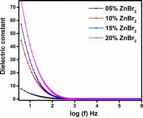
Resin systems formulated for SBU must maintain these properties post-processing, as curing and via formation can alter them. IPC-6012E outlines qualification tests for rigid boards, including dielectric performance verification. Variations in sequential build-up PCB materials can shift characteristic impedance, necessitating simulation adjustments. Thus, selecting dielectrics with proven low Dk and Df ensures reliable high-frequency operation.
Thermal Properties and Their Role in Reliability
Thermal properties govern how sequential build-up PCB materials respond to heat from soldering, power dissipation, or environmental exposure. The glass transition temperature, Tg, marks the point where the material shifts from rigid to rubbery, affecting dimensional stability. Materials with higher Tg resist deformation during reflow, preventing via barrel cracking in SBU layers. Coefficient of thermal expansion, CTE, matching between copper and dielectrics minimizes stress at interfaces, crucial for stacked microvias.
Poor thermal management leads to warpage in asymmetric SBU stack-ups, complicating assembly. Sequential build-up PCB thermal properties like thermal conductivity aid heat spreading, reducing hotspots near high-power components. Factory insights reveal that mismatched CTE causes reliability failures under thermal cycling. Engineers specify materials with balanced Z-axis CTE to core laminates for enhanced durability.
Beyond basic metrics, moisture absorption influences thermal performance, as absorbed water lowers effective Tg and increases loss tangent. Standards like IPC-6012E mandate thermal shock testing to validate material robustness. Optimizing sequential build-up PCB thermal properties extends board lifespan in demanding applications.
Material Interactions in Sequential Build-Up Processes
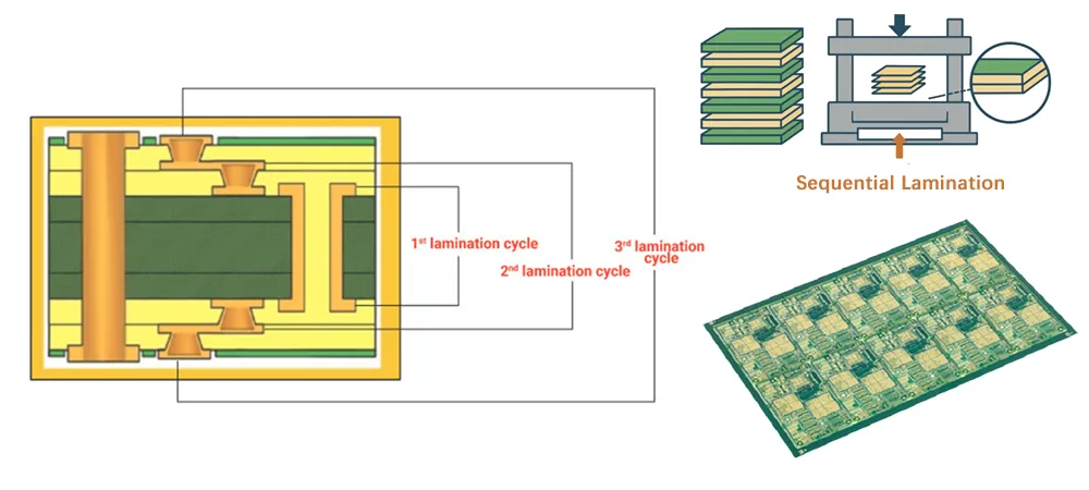
In SBU fabrication, materials interact during sequential lamination, where resin-coated copper foils fill vias and form new dielectrics. Adhesion strength between layers depends on surface treatments and resin chemistry, impacting peel strength. Sequential build-up PCB materials must exhibit low shrinkage during cure to maintain laser-drilled via registration. Factory-driven processes highlight the need for photoimageable dielectrics that support fine features without residue.
Electromechanical coupling arises when thermal expansion differentials strain microvias, potentially causing open circuits. Low-modulus dielectrics absorb stresses better, preserving integrity. Sequential build-up PCB dielectric constant variations from processing can alter controlled impedance stacks. Comprehensive material datasheets guide selections for compatibility.
Best Practices for Material Selection in SBU PCBs
Begin with application requirements: high-speed signals demand low Dk/Df materials, while power-heavy designs prioritize thermal conductivity. Cross-reference sequential build-up PCB materials against IPC-2226 for HDI-specific constraints. Simulate stack-ups to verify impedance and thermal profiles before committing. Collaborate with fabricators early to confirm process compatibility, such as via fill resins.
Layer-specific selection optimizes performance: use low-loss dielectrics near signal layers and high-Tg cores for stability. Balance cost with performance by tiering materials across the stack-up. Conduct design reviews focusing on sequential build-up PCB loss tangent for critical nets. Prototype testing under accelerated conditions validates choices.
Qualification per IPC-6012E ensures production readiness. Document material sets for repeatability. These practices mitigate risks in complex SBU designs.
Practical Insights from Manufacturing Perspectives
Factory experience shows that sequential build-up PCB thermal properties directly influence yield during multiple lamination cycles. Overlooking CTE mismatch often results in bow and twist exceeding tolerances. Sequential build-up PCB materials with enhanced filler content improve thermal dissipation without compromising electricals. Troubleshooting delamination traces back to inadequate resin flow in blind vias.
Optimizing cure profiles preserves sequential build-up PCB dielectric constant stability. Insights from high-volume runs emphasize prepreg selection for uniform thickness control.
Conclusion
Material selection profoundly shapes sequential build-up PCB performance, from electrical fidelity via dielectric constant and loss tangent to reliability through thermal properties. Electrical engineers benefit from structured evaluations aligned with standards like IPC-2226 and IPC-6012E. Best practices in stack-up design and process compatibility yield robust boards. Prioritizing these factors ensures high-density designs excel in demanding applications. Future advancements will refine materials for even tighter tolerances.
FAQs
Q1: What role does sequential build-up PCB dielectric constant play in high-speed designs?
A1: The dielectric constant determines signal velocity and impedance control in sequential build-up PCBs. Lower values enable faster propagation and reduced crosstalk in dense routing. Factory lamination preserves Dk stability, critical per IPC-2226 guidelines. Selecting consistent materials across layers prevents skew in multilayer stacks.
Q2: How does loss tangent affect sequential build-up PCB materials performance?
A2: Loss tangent measures dielectric energy loss, impacting signal attenuation at high frequencies. Low sequential build-up PCB loss tangent materials minimize insertion loss for data integrity. Processing must avoid increasing Df through contamination. Engineers specify based on frequency bands for optimal trace lengths.
Q3: Why are thermal properties vital for sequential build-up PCB materials?
A3: Thermal properties like Tg and CTE ensure stability during reflow and operation in sequential build-up PCBs. Matching prevents via stress and warpage in stacked layers. IPC-6012E tests verify endurance under cycling. Robust materials support reliable HDI fabrication.
Q4: How to select sequential build-up PCB materials for reliability?
A4: Evaluate Dk, Df, Tg, and CTE against application needs and standards like IPC-2226. Simulate thermal-mechanical stresses for stack-ups. Factory validation through prototypes confirms compatibility. Balance electrical and thermal priorities for long-term performance.
References
IPC-2226 — Design Standard for High Density Interconnects. IPC, 2001 (with amendments)
IPC-6012E — Qualification and Performance Specification for Rigid Printed Boards. IPC, 2015
IPC-6016D — Qualification and Performance Specification for High Density Interconnect (HDI) Printed Boards. IPC, 2018





