 ALLPCB


Electronic hobbyists often focus on creating functional circuits and innovative designs. Yet every printed circuit board eventually reaches the end of its useful life. When hobby projects contribute to electronic waste streams, the materials and components embedded in those boards create long-term environmental and health considerations. Responsible approaches to design and disposal help minimize these effects while supporting continued creativity in electronics.
Why Responsible Handling of PCB Waste Matters
Electronic waste from hobby projects includes discarded boards, components, and assemblies that contain metals, plastics, and sometimes hazardous substances. These items add to global e-waste volumes when they are not managed properly. Hobbyists who understand the lifecycle of their creations can make choices that reduce unnecessary accumulation in landfills. Ethical electronics design therefore extends beyond functionality to include end-of-life planning from the initial schematic stage.
The environmental impact of PCBs arises from both the materials used and the difficulty of separating those materials during recycling. Copper traces, fiberglass substrates, solder alloys, and various component packages resist simple breakdown. When boards enter general waste streams, valuable resources are lost and potential contaminants can leach into soil and water. Sustainable hobby electronics practices aim to preserve resources and limit such releases through thoughtful selection of parts and assembly methods.
Mechanisms Behind PCB Contributions to E-Waste
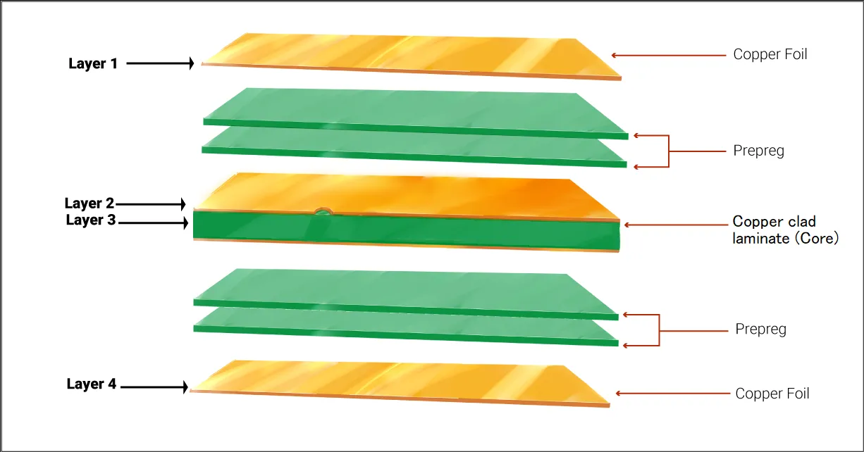
Printed circuit boards combine multiple material layers that serve electrical and mechanical functions. The substrate typically consists of woven glass fibers in an epoxy resin matrix, while conductive paths rely on copper foil. Component attachment uses solder that may contain tin, lead, or lead-free alternatives. Over time, thermal cycling, mechanical stress, and environmental exposure can degrade these assemblies, leading to failure and eventual disposal.
Industry standards such as IPC-6012E guide the qualification of rigid boards and influence material choices that affect recyclability. Boards built to consistent quality levels tend to last longer in service, delaying their entry into waste streams. At the same time, the presence of mixed materials complicates mechanical separation processes used by recyclers. Hobbyists who select components with fewer hazardous constituents help reduce the complexity of downstream handling.
Design decisions also play a role in how easily boards can be disassembled or processed. Dense layouts and permanent adhesives hinder manual separation of parts. Conversely, modular construction and the use of through-hole components in certain applications can facilitate recovery of reusable elements. These engineering considerations directly influence the overall environmental footprint of a finished project.
Best Practices for Ethical Electronics Design and Disposal
Hobbyists can adopt several approaches to limit the e-waste impact of their PCB projects. Selecting components rated for extended temperature ranges or higher reliability often extends operational life. Designing boards with future repair in mind, such as providing test points and accessible connectors, reduces the likelihood of complete replacement. These choices align with principles of ethical electronics design that value longevity over rapid turnover.
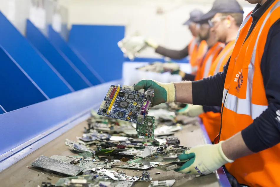
Responsible e-waste disposal begins with identifying local collection programs that accept electronic assemblies. Many regions maintain specialized facilities equipped to handle circuit boards separately from household trash. Hobbyists should avoid mixing boards with general refuse and instead prepare items by removing large batteries or obvious hazardous parts when safe to do so. Documentation of component types used in a project can assist recyclers in determining appropriate processing methods.
Material selection during the design phase further supports sustainable hobby electronics. Preference for lead-free solder alloys and halogen-free laminates, where performance requirements allow, simplifies compliance with environmental expectations. Keeping detailed records of the parts and processes used also helps when evaluating disposal options later. Consistent application of these practices across multiple projects gradually reduces cumulative environmental impact.
Practical Insights for Hobbyists Managing Project Lifecycles
Many hobby projects begin as learning exercises or prototypes that may be superseded by improved versions. Tracking the intended duration of use helps determine whether a board should be built for maximum durability or for easier eventual recycling. In cases where a design is experimental, using readily available standard parts rather than specialized components can improve the chances of material recovery. Such forward-looking decisions embody the core of responsible e-waste disposal.
Testing and validation steps recommended by standards such as IPC-A-600K help ensure boards meet basic quality thresholds before they enter service. Boards that pass visual and dimensional acceptance criteria are less likely to fail prematurely. This reduces the frequency of replacements and the associated waste generation. Hobbyists who incorporate these checks into their workflow gain both functional reliability and environmental benefits.
Conclusion
The ethics of e-waste in hobby electronics require attention to material choices, design longevity, and proper end-of-life handling. By understanding how PCBs contribute to waste streams and applying consistent best practices, hobbyists can maintain creative output while limiting environmental consequences. Standards from organizations such as IPC provide useful frameworks for quality that indirectly support sustainability goals. Continued awareness of these factors strengthens the overall responsibility of the electronics hobby community.
FAQs
Q1: What is the e-waste impact of typical PCB projects?
A1: Hobbyist printed circuit boards contribute to electronic waste through their combination of metals, resins, and components that are difficult to separate once discarded. When boards enter landfills, valuable resources are lost and potential contaminants may affect surrounding environments. Ethical electronics design encourages longer service life and selection of materials that facilitate later recovery.
Q2: How can hobbyists practice responsible e-waste disposal?
A2: Responsible e-waste disposal involves using designated collection points that handle electronic assemblies rather than placing boards in regular trash. Preparing items by removing batteries and noting material types assists specialized recyclers. Consistent habits across projects help reduce the overall volume of hobby-related waste.
Q3: What role does sustainable hobby electronics play in reducing environmental impact?
A3: Sustainable hobby electronics focuses on design choices that extend product life and simplify material recovery at end of life. Selecting reliable components and avoiding unnecessary complexity lowers the frequency of replacements. These approaches directly address the environmental impact of PCBs by conserving resources and limiting waste generation.
Q4: Why should electronic hobbyists consider ethical electronics design?
A4: Ethical electronics design incorporates end-of-life considerations from the start, leading to boards that last longer and create fewer disposal challenges. This mindset aligns personal creativity with broader environmental responsibility. Over time, such practices help minimize the cumulative e-waste impact of PCB projects.
References
IPC-6012E — Qualification and Performance Specification for Rigid Printed Boards. IPC, 2017
IPC-A-600K — Acceptability of Printed Boards. IPC, 2020
JEDEC J-STD-020E — Moisture/Reflow Sensitivity Classification. JEDEC, 2014


