 ALLPCB


Introduction
Printed circuit boards form the backbone of modern electronics, enabling everything from consumer devices to industrial systems. The etching process, a critical step in PCB manufacturing, selectively removes excess copper to define circuit patterns. However, traditional etching methods generate significant environmental challenges, including hazardous chemical waste and heavy metal contamination. As regulatory pressures mount and sustainability becomes a priority in sustainable PCB manufacturing, engineers must explore ways to mitigate the PCB etching environmental impact. This article examines these issues, highlights eco-friendly PCB etching strategies, and discusses alternative etchants alongside waste reduction techniques. Factory-driven insights reveal how aligning processes with environmental goals enhances both compliance and efficiency.
What Is PCB Etching and Why Does Its Environmental Impact Matter?
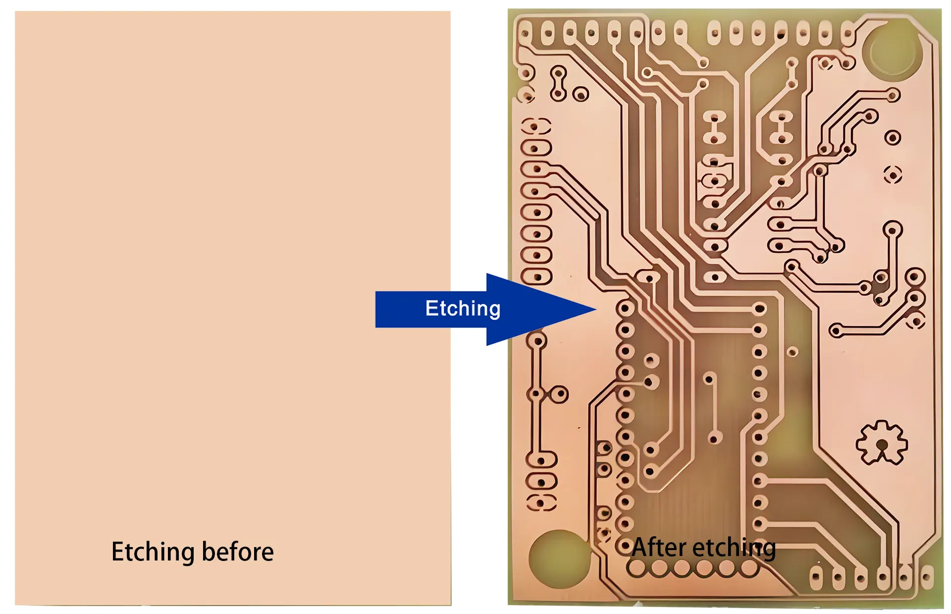
PCB etching involves exposing a copper-clad laminate to a chemical etchant after applying a resist mask to protect desired traces. Common etchants dissolve unprotected copper, creating the conductive pathways essential for electrical performance. This process occurs in controlled tanks with agitation to ensure uniform etching rates and minimize undercutting. While vital for high-volume production, etching contributes to environmental strain through spent solutions laden with dissolved copper and other byproducts.
The PCB etching environmental impact stems primarily from wastewater discharge and solid waste generation. Copper ions in effluent pose toxicity risks to aquatic life, while acidic or alkaline residues disrupt pH balances in treatment systems. High water consumption for rinsing further exacerbates resource use in water-scarce regions. For electric engineers, understanding these effects is crucial, as they influence material selection, process design, and compliance with global regulations. Sustainable PCB manufacturing demands addressing these issues to reduce long-term ecological footprints without compromising board quality.
Technical Principles of Traditional PCB Etching and Key Environmental Concerns
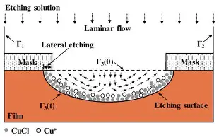
Traditional etchants like ferric chloride oxidize copper to form soluble copper chloride complexes, with iron reducing from Fe3+ to Fe2+. The reaction proceeds as panels move through etching chambers, where spray or immersion ensures contact. Spent etchant accumulates copper, slowing the reaction and necessitating replacement, which generates large volumes of hazardous waste. Regeneration attempts often fail due to iron buildup, leading to sludge formation during neutralization.
Ammonium persulfate offers an alternative acidic etchant, breaking down into sulfate radicals that attack copper surfaces. Alkaline etching with cupric chloride maintains a chloride-rich environment, where Cu2+ ions etch copper while forming Cu+ intermediates. Each method produces distinct wastes: acidic processes yield metal-laden sludge, while alkaline ones require careful ammonia management to prevent volatilization. Energy demands from heating and pumping add to the carbon footprint. These mechanisms highlight why waste reduction in PCB manufacturing remains a factory priority.
Air emissions from volatile organics in resists or fumes during etching further compound impacts, though modern enclosures mitigate this. Solid wastes include filter cakes from precipitation, often classified as hazardous due to heavy metal content. Water usage can exceed thousands of liters per panel in rinse cycles, straining municipal systems. Engineers must balance etch factor, uniformity, and sidewall control against these environmental costs.
Detailed Environmental Impacts of PCB Etching
Water pollution represents the most pressing concern, with copper concentrations in effluent often exceeding discharge limits. Untreated discharge leads to bioaccumulation in food chains, affecting fisheries and drinking water sources. Acidic etchants lower pH, harming microbial activity in sewage treatment plants. Factory data shows that without treatment, a single production line can release tons of copper annually.
Solid waste from neutralization forms copper hydroxide precipitates, requiring landfilling or specialized disposal. These sludges occupy landfill space and pose leaching risks over time. Energy consumption for etchant heating, typically to 40-50°C, contributes to greenhouse gas emissions, especially in fossil-fuel-dependent facilities. Noise and odor from ventilation systems add localized impacts, though less severe than chemical releases.
Cumulative effects amplify across the supply chain, where global PCB production scales these issues exponentially. Engineers evaluating designs should consider etching's role in total lifecycle assessments, prioritizing processes that align with environmental management frameworks.
Sustainable Practices for Eco-Friendly PCB Etching
Implementing closed-loop etchant systems regenerates solutions by electrolytic oxidation, converting Cu+ back to Cu2+ while harvesting pure copper at the cathode. Filtration removes particulates, extending etchant life cycles and slashing waste volumes. Precise chemistry control via inline sensors maintains optimal Cu2+/Cl- ratios, preventing premature degradation. These factory practices achieve substantial waste reduction in PCB manufacturing by minimizing fresh etchant inputs.
Compliance with ISO 14001 standards guides environmental management, emphasizing pollution prevention and continual improvement. Factories integrate ISO 14001 principles through etchant recovery plants that precipitate copper selectively, yielding saleable metal while neutralizing residuals. Rinse water recycling via ion exchange or reverse osmosis cuts usage by recycling 80-90% back to production. pH adjustment and sedimentation precede discharge, ensuring regulatory compliance.
Multistage rinsing with counterflow reduces drag-out, where panels carry etchant to subsequent tanks. Automation optimizes spray patterns, reducing over-etching and chemical overuse. Operator training on spill containment and housekeeping prevents incidental releases. These measures not only curb PCB etching environmental impact but also lower operational costs through resource efficiency.
Alternative Etchants and Emerging Methods
Cupric chloride etchant supports regeneration more readily than ferric chloride, as air sparging oxidizes Cu+ without iron contamination. Its alkaline nature allows tin resists, compatible with fine-line features down to 50 microns. Hydrogen peroxide-sulfuric acid mixtures generate etchants in situ, producing less sludge since copper sulfate precipitates controllably. These alternatives promote eco-friendly PCB etching by enabling higher regeneration rates.
Persulfate-based etchants decompose to benign sulfates, easing neutralization compared to chlorides. However, they require stabilizers to prevent auto-decomposition, and copper recovery demands chelation. Electrochemical etching uses anodic dissolution, minimizing bulk chemicals through localized reactions at the panel surface. Plasma or laser ablation offers dry alternatives, though scalability limits high-volume use.
Factory trials favor hybrid systems combining chemical etching with inline regeneration. Engineers select based on line width, throughput, and waste profiles. IPC-1401 provides guidelines for managing emissions from etching processes, supporting transitions to lower-impact options.
Best Practices for Waste Reduction in Production
Panel racking minimizes drag-out by optimizing dwell times and squeegee bars. Etch factor control via conveyor speed and nozzle pressure prevents excess copper removal, conserving etchant. Spent solution monitoring triggers regeneration before saturation, avoiding dumps. Copper recovery via electrowinning yields 99% pure metal, offsetting costs.
Integration of ISO 14001 auditing ensures practices evolve with technology. Cross-contamination avoidance through dedicated lines preserves etchant purity. These factory-driven strategies deliver measurable gains in sustainable PCB manufacturing.
Conclusion
PCB etching's environmental toll, from heavy metal wastes to high water use, demands proactive mitigation. Closed-loop regeneration, alternative etchants like cupric chloride, and adherence to standards such as ISO 14001 transform challenges into opportunities for efficiency. Electric engineers play a pivotal role by specifying compatible designs and advocating waste reduction in PCB manufacturing. Adopting these practices fosters eco-friendly PCB etching, ensuring industry growth aligns with planetary health. Future innovations promise even greener processes, balancing performance with responsibility.
FAQs
Q1: What are the main contributors to PCB etching environmental impact?
A1: Traditional etchants like ferric chloride generate copper-rich wastewater, acidic sludge, and high rinse water volumes, leading to aquatic toxicity and resource strain. Factory mitigation focuses on regeneration to minimize discharge. Sustainable PCB manufacturing integrates these controls for compliance and efficiency.
Q2: How do closed-loop systems support waste reduction in PCB manufacturing?
A2: Closed-loop etching regenerates solutions via electrolysis, recovers copper, and recycles rinse water, cutting fresh chemical needs by significant margins. This aligns with ISO 14001 for pollution prevention. Electric engineers benefit from stable processes and lower disposal costs.
Q3: What alternative etchants offer eco-friendly PCB etching options?
A3: Cupric chloride and persulfate etchants enable regeneration with fewer toxic byproducts than ferric chloride. Hydrogen peroxide mixtures reduce sludge formation. Selection depends on resolution and throughput requirements in production.
Q4: Why reference standards like ISO 14001 in sustainable PCB manufacturing?
A4: ISO 14001 provides frameworks for environmental management, guiding waste handling and process optimization in etching. It ensures continual improvement and regulatory alignment. Factories use it to benchmark eco-friendly PCB etching progress.


