ALLPCB


Why Trace Width and Spacing Matter in HDI PCBs
High-density interconnect (HDI) printed circuit boards enable compact, high-performance electronic systems by packing more functionality into smaller areas. Engineers face increasing pressure to optimize trace width and spacing while maintaining manufacturability and electrical performance. Design for manufacturability (DFM) principles guide these decisions to reduce defects, improve yield, and ensure reliable operation in demanding applications. Effective management of trace parameters directly influences signal integrity, thermal behavior, and overall board reliability. This article examines the engineering considerations and strategies that support successful HDI PCB implementation.
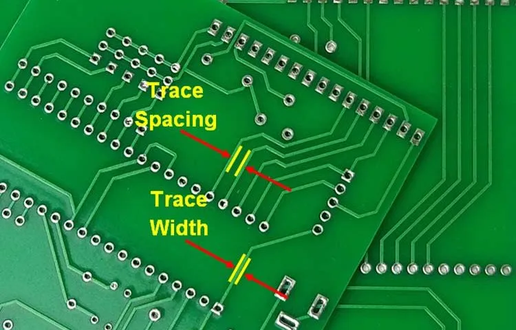
Trace width and spacing define the conductive paths on a PCB and determine how signals propagate between components. In HDI designs, finer features allow greater routing density but introduce tighter tolerances during fabrication and assembly. Insufficient spacing can lead to short circuits or excessive crosstalk, while overly narrow traces may increase resistance and heat generation. Proper dimensioning supports impedance matching and minimizes electromagnetic interference in high-speed circuits. These factors collectively affect production costs, time to market, and long-term product reliability for engineers working on complex systems.
Technical Principles of Trace Width Calculation and Spacing Rules
Trace width calculation in HDI PCBs begins with current-carrying requirements, voltage isolation needs, and thermal dissipation limits. Engineers apply established formulas that relate conductor cross-section to maximum allowable temperature rise under load. Spacing rules derive from dielectric strength considerations and manufacturing process capabilities, ensuring adequate insulation between adjacent traces. In high-density layouts, these parameters interact with via placement and layer stack-up to influence overall board performance. Signal integrity analysis further refines these values by accounting for propagation delay and reflection characteristics.
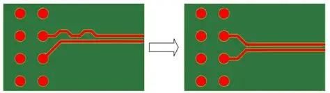
Impedance control trace width becomes critical when designing transmission lines for high-frequency signals. Controlled impedance requires precise calculation of trace geometry relative to the surrounding dielectric materials and reference planes. Deviations in width or spacing alter the characteristic impedance, leading to mismatches that degrade signal quality. Differential pair routing DFM extends these principles by maintaining consistent spacing and length matching between paired conductors. This approach preserves signal balance and reduces susceptibility to common-mode noise in high-density PCB environments.
Design Rules and Signal Integrity Considerations
Signal integrity in high-density PCBs depends on minimizing discontinuities that arise from improper trace dimensions. Crosstalk between adjacent traces increases when spacing falls below recommended thresholds, coupling unwanted energy into neighboring signals. Engineers evaluate these effects through simulation and apply spacing rules that scale with operating frequency and edge rates. Trace width also influences skin effect losses at higher frequencies, where current concentrates near the conductor surface. Balancing these factors requires iterative refinement during the layout phase to achieve acceptable noise margins.
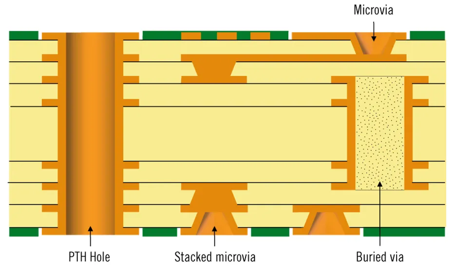
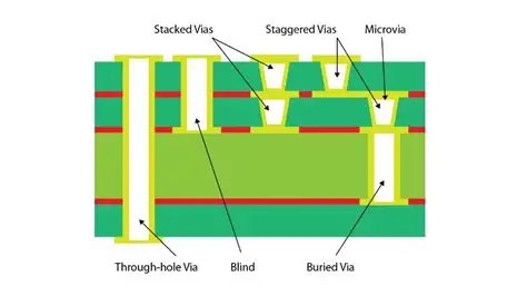
Manufacturing constraints further shape design rules for trace width and spacing. Etching processes impose minimum feature sizes and tolerances that vary with copper thickness and board material. HDI fabrication often incorporates sequential lamination and laser-drilled microvias, which interact with trace routing to affect yield. Adherence to standardized design guidelines helps align layout intent with process capabilities. This alignment reduces the need for costly rework and supports consistent electrical performance across production batches.
DFM Strategies for Trace Width and Spacing Optimization
Design for manufacturability begins with early collaboration between layout engineers and fabrication teams to establish feasible trace parameters. Standard spacing rules typically incorporate safety margins beyond minimum electrical requirements to accommodate process variations. Trace width calculation incorporates both functional current needs and manufacturing allowances for etching undercut. Implementing these strategies early in the design cycle prevents downstream issues during prototyping and volume production.
Impedance control trace width optimization involves selecting appropriate stack-up configurations and verifying dimensions against target values. Engineers often employ test coupons on production panels to validate impedance after fabrication. Differential pair routing DFM emphasizes uniform spacing along the entire pair length while avoiding abrupt changes in reference planes. These practices enhance signal integrity high density PCB performance by reducing reflections and maintaining consistent transmission characteristics. Regular design rule checks integrated into the workflow catch violations before they propagate into manufacturing.
Additional considerations include thermal management through adequate trace sizing and strategic placement of copper pours for heat spreading. In dense areas, engineers may adjust spacing locally to accommodate thermal relief patterns around vias without compromising electrical isolation. Documentation of all trace parameters supports traceability and facilitates troubleshooting during qualification testing.
Conclusion
Effective management of trace width and spacing forms a cornerstone of successful HDI PCB design. By integrating DFM principles with electrical requirements, engineers achieve reliable signal integrity while supporting high manufacturing yields. Structured application of calculation methods and spacing rules reduces risks associated with high-density layouts. Ongoing attention to these parameters throughout the design process delivers boards that meet both performance targets and production realities.
FAQs
Q1: How does trace width calculation HDI PCB influence current carrying capacity?
A1: Trace width calculation in HDI PCBs determines the conductor cross-section needed to handle specified currents without excessive temperature rise. Engineers factor in copper thickness, ambient conditions, and allowable heating to arrive at minimum dimensions. This approach prevents thermal degradation while fitting within the constraints of dense interconnect layers.
Q2: What are the key trace spacing design rules HDI PCB for avoiding crosstalk?
A2: Trace spacing design rules in HDI PCBs establish minimum distances between conductors based on voltage levels and signal frequencies. Adequate spacing limits capacitive and inductive coupling that can degrade signal quality. These rules scale with operating conditions to maintain acceptable noise performance in compact layouts.
Q3: Why is impedance control trace width important in high-speed designs?
A3: Impedance control trace width ensures transmission lines match the characteristic impedance required by connected components. Precise geometry relative to dielectric thickness and reference planes minimizes reflections and preserves signal fidelity. This control becomes essential as data rates increase in high-density PCB applications.
Q4: How does differential pair routing DFM improve signal integrity high density PCB performance?
A4: Differential pair routing DFM maintains consistent spacing and length equality between paired traces to preserve signal balance. This technique reduces susceptibility to external noise and common-mode interference in dense environments. Proper implementation supports reliable data transmission in space-constrained HDI designs.
References
IPC-2221B — Generic Standard on Printed Board Design. IPC, 2012
IPC-6012E — Qualification and Performance Specification for Rigid Printed Boards. IPC, 2017
IPC-A-600K — Acceptability of Printed Boards. IPC, 2020