ALLPCB


In the fast-growing world of Internet of Things (IoT) devices, single-sided PCBs (Printed Circuit Boards) play a vital role due to their simplicity and cost-effectiveness. However, designing and using single-sided PCB IoT applications comes with unique challenges like space constraints, power consumption, and connectivity issues. The good news? There are practical solutions to overcome these hurdles, ensuring reliable performance for IoT sensors, wireless systems, and more. In this blog, we’ll explore the specific challenges of using single-sided PCBs in IoT devices and provide actionable solutions to help engineers and designers succeed.
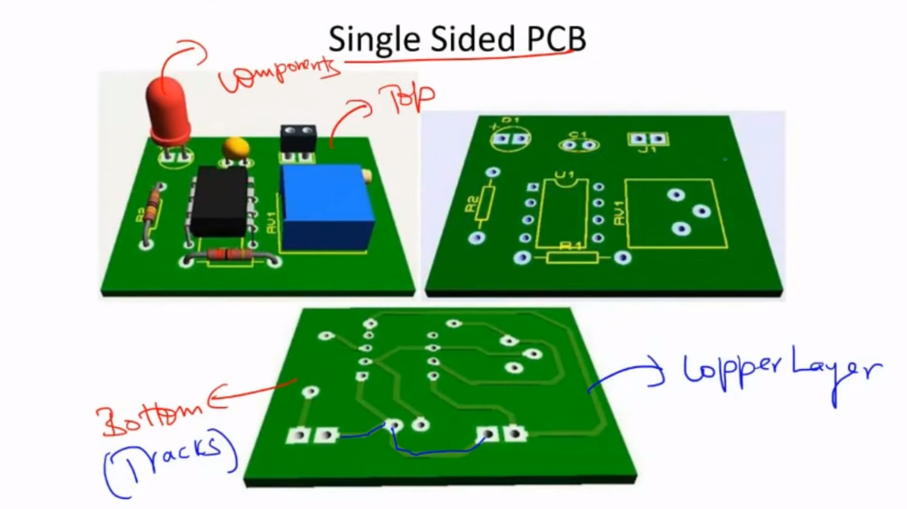
What Are Single-Sided PCBs and Their Role in IoT?
Single-sided PCBs are circuit boards with conductive traces on only one side, making them a budget-friendly and straightforward option for many electronic designs. In the realm of IoT, these boards are often used in compact devices like sensors, wearable gadgets, and smart home products due to their low cost and ease of manufacturing. Their simplicity suits applications where complex multi-layer designs are unnecessary.
IoT devices, such as smart thermostats or fitness trackers, rely on single-sided PCBs to connect basic components like microcontrollers, sensors, and power management circuits. However, as IoT systems become more advanced, the limitations of single-sided PCBs can create obstacles. Let’s dive into the key challenges and how to address them for optimal performance in single-sided PCB IoT applications.
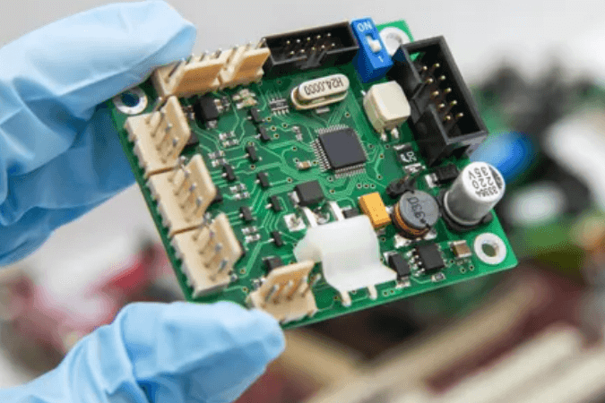
Key Challenges of Single-Sided PCBs in IoT Devices
While single-sided PCBs are affordable and easy to produce, they pose several challenges when used in IoT systems. These challenges often revolve around space, power, connectivity, and signal integrity. Below, we break down the most common issues faced by engineers working on single-sided PCB IoT sensors and other applications.
1. Limited Space for Complex Designs
IoT devices are typically small, requiring compact PCB layouts. Single-sided PCBs, with traces only on one side, offer limited routing space. This can be a significant problem when integrating multiple components like sensors, wireless modules, and microcontrollers. Overcrowding often leads to messy layouts, increasing the risk of interference or manufacturing errors.
2. Power Consumption Constraints
Energy efficiency is critical for IoT devices, especially battery-powered ones like wearable sensors or remote monitoring systems. Single-sided PCB IoT power consumption challenges arise because these boards may not support advanced power management circuits due to space limitations. Inefficient power delivery can result in higher energy usage, shortening battery life. For instance, a poorly designed power trace might cause a voltage drop, reducing efficiency by up to 10-15% in some cases.
3. Wireless Connectivity Issues
Many IoT devices rely on wireless technologies like Wi-Fi, Bluetooth, or Zigbee for communication. Designing effective antenna layouts and ensuring signal integrity on a single-sided PCB is tough. Single-sided PCB IoT wireless systems often suffer from signal interference due to the inability to create proper ground planes or shielding on a single layer. This can lead to reduced range or dropped connections, with signal loss sometimes reaching 20% or more compared to multi-layer designs.
4. Signal Integrity and Noise
With all traces on one side, single-sided PCBs are prone to crosstalk and electromagnetic interference (EMI). This is especially problematic for IoT sensors that require precise data readings. For example, a temperature sensor on a single-sided PCB might pick up noise from nearby power traces, leading to inaccurate readings with deviations of up to 2-3°C.
5. Durability and Reliability
IoT devices are often deployed in varied environments, from industrial settings to outdoor applications. Single-sided PCBs, lacking the structural support of additional layers, are more vulnerable to physical stress, heat, and humidity. This can result in trace damage or component failure over time, with failure rates potentially increasing by 5-10% in harsh conditions compared to multi-layer boards.
Solutions for Single-Sided PCB Challenges in IoT
Despite these challenges, single-sided PCBs can still be a viable choice for IoT devices with the right strategies. Below, we outline practical solutions to address the limitations and ensure reliable performance for single-sided PCB IoT sensors, wireless systems, and more.
1. Optimizing Layout Design for Space Efficiency
To tackle space constraints, careful planning of the PCB layout is essential. Use design software to strategically place components and traces, minimizing overlap and interference. Prioritize placing high-priority components like microcontrollers and sensors first, then route power and signal traces around them. For instance, grouping related components together can reduce trace length by up to 30%, freeing up space and reducing noise.
Another tip is to use surface-mount components (SMDs) instead of through-hole parts. SMDs are smaller and allow for denser layouts, making them ideal for compact IoT devices. Additionally, consider using zero-ohm resistors as jumpers to cross traces without needing a second layer.
2. Reducing Power Consumption with Efficient Design
For single-sided PCB IoT power consumption issues, focus on optimizing power delivery. Use wider traces for power lines to minimize resistance and voltage drops—aim for a trace width of at least 0.5mm for currents up to 1A. Incorporate low-power components, such as microcontrollers with sleep modes, to cut energy use during idle periods. For example, switching to a low-power mode can reduce consumption by 50-70% in some IoT sensors.
Adding simple power management circuits, like voltage regulators with high efficiency (above 85%), can also help. Place decoupling capacitors close to power-hungry components to stabilize voltage and reduce noise, ensuring consistent performance.
3. Enhancing Wireless Performance
Improving single-sided PCB IoT wireless connectivity requires careful antenna design and placement. Keep antenna traces short and straight, avoiding sharp bends that can degrade signal quality. If possible, reserve a clear area around the antenna to minimize interference from other components. For Bluetooth modules, maintain a keep-out zone of at least 5mm around the antenna to achieve optimal range, potentially boosting signal strength by 10-15%.
Since single-sided PCBs lack a full ground plane, create a pseudo-ground area by filling unused spaces with copper connected to ground. This can reduce EMI and improve wireless performance, even if it’s not as effective as a multi-layer ground plane.
4. Minimizing Signal Noise and Interference
To address signal integrity, separate high-speed signal traces from power lines by at least 0.3mm to prevent crosstalk. Route critical sensor signals, like those from temperature or pressure sensors, away from noisy components. If noise persists, consider adding small ferrite beads or filters near sensitive components to suppress high-frequency interference, reducing noise levels by up to 20% in some designs.
For IoT devices requiring precise data, test the PCB layout under real-world conditions to identify and fix interference issues early. Simulation tools can also predict potential noise problems before manufacturing, saving time and cost.
5. Improving Durability for Harsh Environments
To enhance the reliability of single-sided PCBs in tough conditions, apply a conformal coating to protect against moisture and dust. A coating thickness of 25-50 micrometers can increase resistance to environmental stress by up to 30%. Use high-quality materials for the PCB substrate, such as FR-4 with a high glass transition temperature (Tg) of 130°C or more, to withstand heat.
Additionally, reinforce mounting points and secure components with adhesives to prevent damage from vibrations. For outdoor IoT devices, ensure proper enclosure design to shield the PCB from direct exposure to elements, extending lifespan significantly.
Advantages of Single-Sided PCBs in IoT Applications
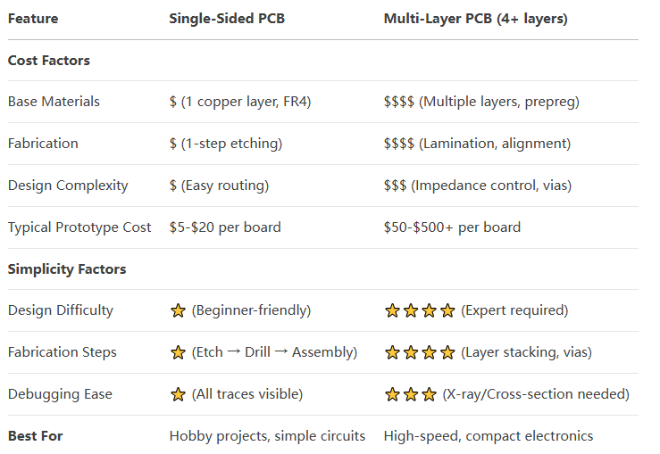
Despite the challenges, single-sided PCBs offer distinct benefits that make them suitable for many IoT projects. Their low production cost—often 20-40% cheaper than double-sided or multi-layer boards—makes them ideal for mass-produced, cost-sensitive devices like basic sensors or smart home gadgets. Manufacturing is also faster and simpler, with fewer steps involved, reducing lead times by up to 25% in some cases.
Moreover, their simplicity aids in troubleshooting and repairs, as all traces are visible on one side. This can cut down maintenance time by 15-20% compared to complex multi-layer designs, a significant advantage for IoT devices deployed in large numbers.
Best Practices for Designing Single-Sided PCBs for IoT
To maximize the potential of single-sided PCBs in single-sided PCB IoT applications, follow these best practices:
- Prioritize Component Placement: Place critical components first and route traces logically to avoid congestion.
- Use Simulation Tools: Test layouts virtually to spot issues like noise or power inefficiencies before production.
- Focus on Power Efficiency: Select low-power components and optimize trace widths for minimal energy loss.
- Plan for Scalability: Design with future upgrades in mind, leaving room for additional components if needed.
- Test Under Real Conditions: Validate the PCB in environments similar to its intended use to ensure reliability.
Conclusion: Balancing Cost and Performance with Single-Sided PCBs
Single-sided PCBs are a valuable choice for IoT devices, offering affordability and simplicity for applications like sensors and wireless systems. While challenges like limited space, single-sided PCB IoT power consumption, and connectivity issues exist, they can be addressed with smart design practices and innovative solutions. By optimizing layouts, enhancing power efficiency, and improving signal integrity, engineers can create reliable and effective IoT solutions using single-sided PCBs.
Whether you’re designing single-sided PCB IoT sensors or wireless modules, the key is to balance cost with performance. With the right approach, these boards can power the next generation of connected devices, driving innovation in the IoT space. Partnering with a trusted PCB manufacturing service can further streamline the process, ensuring high-quality results tailored to your needs.