 ALLPCB


Introduction
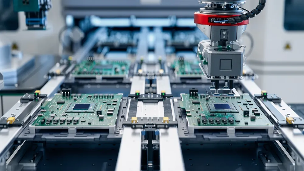
Single-sided printed circuit boards represent the simplest form of PCB construction, featuring conductive traces and components on only one side of the substrate. These boards find applications in basic consumer electronics, sensors, and control systems where complex routing is unnecessary. As environmental concerns grow in the electronics industry, engineers evaluate PCB types based on their lifecycle impacts, from material selection to end-of-life disposal. Single-sided PCBs emerge as a potential sustainable option due to reduced material usage and manufacturing complexity. This article examines their environmental advantages, focusing on eco-friendly materials, recycling processes, and sustainable practices aligned with industry standards. Factory insights reveal how these boards minimize waste while meeting performance needs for electric engineers.
What Is a Single-Sided PCB and Why Does It Matter for Sustainability?
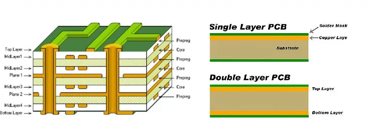
A single-sided PCB consists of a single layer of copper foil laminated onto a non-conductive substrate, typically with a solder mask and silkscreen on the component side. Unlike double-sided or multilayer boards, it lacks vias or inner layers, limiting it to simple circuits but enabling straightforward fabrication. This design suits low-density interconnects in devices like LED displays, calculators, and automotive sensors. Sustainability matters because PCB production consumes significant resources, including energy, water, and chemicals, contributing to electronic waste challenges. Single-sided boards address these by requiring fewer raw materials and simpler processes, potentially lowering the overall environmental footprint. For electric engineers, selecting such boards supports compliance with environmental management systems while optimizing costs.
The relevance intensifies with global e-waste volumes exceeding 50 million tons annually, much from complex electronics. Simpler boards like single-sided types facilitate better resource recovery at recycling facilities. Factory-driven data shows they use up to half the copper of double-sided equivalents for similar footprints. Engineers benefit from reliable performance under IPC standards for rigid boards, ensuring quality without excess layers.
Technical Principles Behind Single-Sided PCB Environmental Impact
The environmental impact of single-sided PCBs stems from their basic structure, which reduces material inputs during fabrication. Copper etching occurs on one side only, minimizing etchant waste compared to multilayer boards with multiple patterning steps. Substrate materials, often epoxy-based laminates, form a thin core without prepregs for lamination, cutting resin and glass fiber consumption. This simplicity lowers energy demands in pressing and drilling, as no through-holes require plating. Thermal processing remains basic, avoiding high-temperature multilayer bonding that increases greenhouse gas emissions. Overall, these factors contribute to a smaller single-sided PCB environmental impact throughout production.
Key mechanisms include optimized copper utilization, where trace widths adhere to design rules without redundant layers. Surface finishes like HASL or ENIG apply selectively, reducing precious metal usage. Factory processes emphasize closed-loop water systems for rinsing, further mitigating pollution. Compared to multilayer PCBs, single-sided variants generate less scrap from panelization inefficiencies. Engineers note that warpage control follows IPC guidelines, maintaining flatness with minimal reinforcement. These principles align with sustainable goals by prioritizing efficiency.
Single-Sided PCB Eco-Friendly Materials and Their Role
Selecting single-sided PCB eco-friendly materials begins with halogen-free laminates that avoid brominated flame retardants, reducing toxicity in production and disposal. Substrates like standard FR-4 grades meet flame retardancy per UL 94 V-0 while supporting recyclability. Copper foil thickness, typically 1 oz/ft2, suffices for low-current designs, conserving metal resources. Solder masks formulated without volatile organic compounds minimize emissions during curing. These choices enable compliance with RoHS directives indirectly through material purity. Factory experience confirms that such materials maintain dielectric strength and thermal conductivity for reliable operation.
Integrating bio-based resins or recycled fibers into substrates enhances sustainability without compromising mechanical properties. Engineers verify compatibility via CTE matching to copper, preventing delamination. Thinner boards reduce overall mass, easing transportation emissions. Material traceability ensures supply chain transparency, a key for ISO-certified facilities. These eco-friendly options prove viable for volume production, balancing performance and planetary health.
Sustainable Manufacturing Processes for Single-Sided PCBs
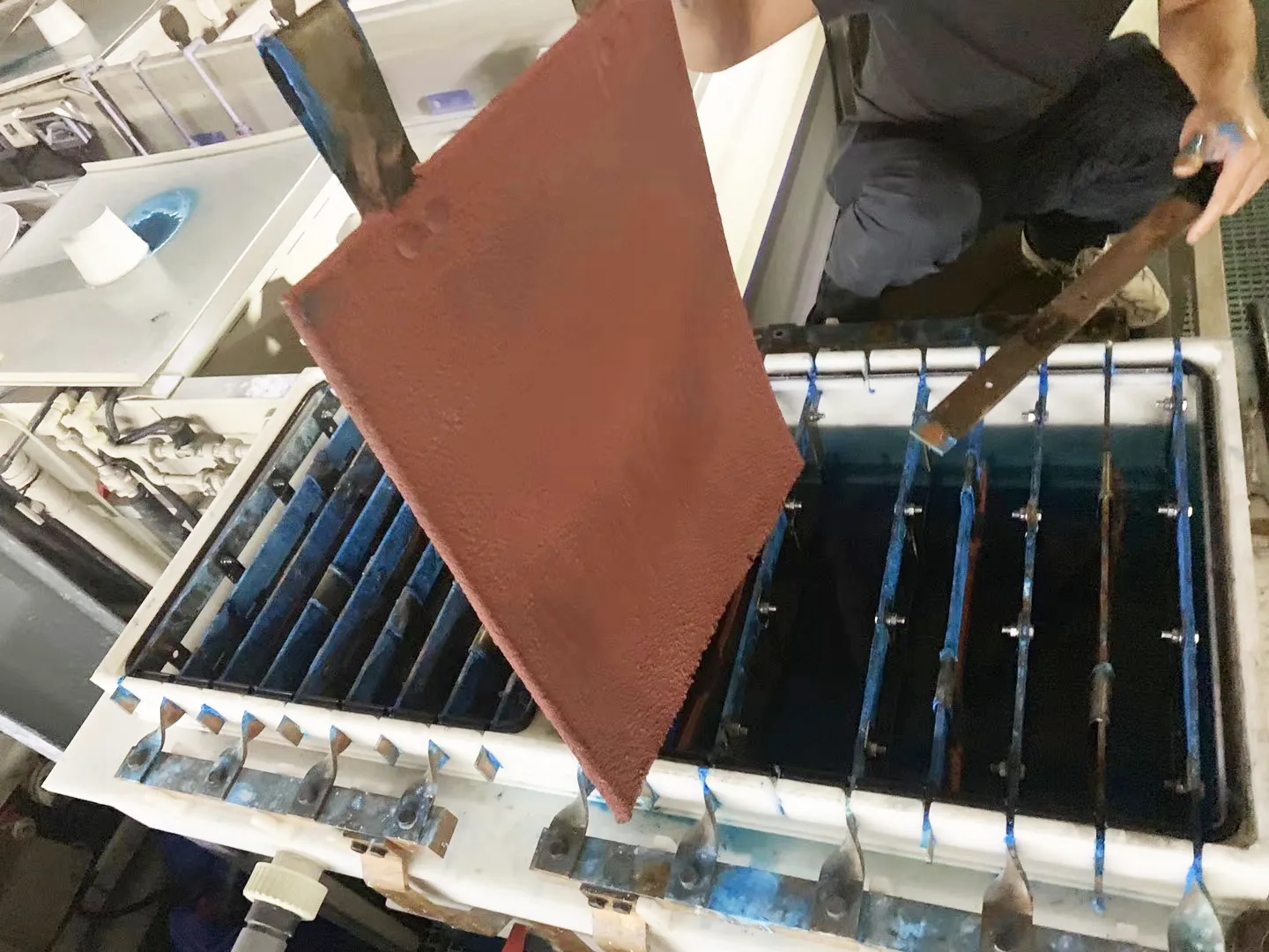
Sustainable manufacturing of single-sided PCBs focuses on streamlined workflows that cut energy and chemical use. Panel preparation involves dry film photoresist application followed by single-sided exposure and development, avoiding multi-step alignments. Etching tanks recycle solutions via ion exchange, recovering copper for reuse. Drilling limits to non-plated holes, slashing slurry waste from abrasive processes. Baking and profiling use efficient ovens with heat recovery systems. These practices embody single-sided PCB sustainable manufacturing by integrating waste minimization from the outset.
Adherence to IPC-A-600 for acceptability ensures defect-free boards without rework, saving resources. Factories implement lean layouts to reduce material handling distances and forklift emissions. Electrical testing employs bed-of-nails fixtures optimized for single-layer nets, speeding throughput. Post-process cleaning relies on deionized water cascades with filtration loops. Engineers appreciate how these methods scale for prototypes to high volumes while tracking carbon footprints.
Single-Sided PCB Recycling Process and Advantages
The single-sided PCB recycling process starts with mechanical dismantling to remove components, leveraging the board's simplicity for quick desoldering. Shredding follows, producing uniform particles from the single copper layer and substrate. Magnetic separation isolates ferrous parts, while eddy currents recover non-ferrous metals like copper efficiently. Density-based flotation divides epoxy resin from fillers, yielding sortable fractions. Pyrolysis or hydrometallurgy refines metals further, with glass fibers reusable in composites. This straightforward flow contrasts with multilayer recycling, where interlayer separation demands more energy.
Advantages include higher yield from uncontaminated copper foil, as no inner layers complicate extraction. Factory recyclers report easier handling due to uniform thickness. Non-metallic residues find applications in construction fillers, closing loops. Engineers design for recyclability by avoiding mixed finishes, aiding purity. ISO 14001 frameworks guide facilities in auditing these processes for continual improvement. Overall, single-sided boards support circular economy principles effectively.
Best Practices for Minimizing Environmental Impact
Engineers adopt design rules maximizing panel utilization, such as tight spacing per IPC-6011, to reduce per-unit material. Simulate thermal profiles early to select minimal copper weights, avoiding over-specification. Specify lead-free assemblies compatible with single-sided constraints. Partner with factories using renewable energy for lamination-free processes. Track lifecycle assessments qualitatively, focusing on layer count reductions. Implement modular designs allowing board reuse in low-complexity upgrades.
Prototyping emphasizes thin substrates to cut mass without strength loss. Validate via thermal cycling tests aligned with J-STD-020 for reliability. Waste audits during pilot runs identify optimization points. These practices ensure single-sided PCBs deliver on sustainability promises.
Conclusion
Single-sided PCBs offer tangible sustainability benefits through reduced materials, simpler manufacturing, and efficient recycling. Their environmental impact proves lower than complex alternatives, suiting applications where performance aligns with simplicity. Factory insights underscore adherence to standards like IPC-A-600 and ISO 14001 for quality and eco-responsibility. Electric engineers gain from cost savings and compliance ease. As electronics evolve, prioritizing such boards fosters greener supply chains. Future designs will build on these foundations for broader adoption.
FAQs
Q1: What materials make single-sided PCB eco-friendly materials viable for production?
A1: Single-sided PCB eco-friendly materials include halogen-free FR-4 laminates and thin copper foils that meet flame retardancy without toxic additives. These support standard processes while enabling easier separation in recycling. Factories select them for compatibility with IPC guidelines, ensuring dielectric integrity. Engineers verify via qualification tests for CTE and moisture absorption.
Q2: How does the single-sided PCB recycling process differ from multilayer boards?
A2: The single-sided PCB recycling process involves shredding a uniform single-layer structure, simplifying magnetic and eddy current separation of copper. Multilayer variants require additional delamination steps, increasing energy use. This efficiency boosts metal recovery rates in factory operations. Standards like ISO 14001 guide waste handling for minimal emissions.
Q3: What is the single-sided PCB environmental impact during manufacturing?
A3: Single-sided PCB environmental impact arises mainly from etching and substrate lamination, but remains lower due to no via plating or multi-press cycles. Closed-loop systems recycle etchants and water effectively. Compared to multilayer, it cuts energy by simplifying steps. IPC-6011 ensures performance without excess resources.
Q4: How can engineers implement single-sided PCB sustainable manufacturing?
A4: Implement single-sided PCB sustainable manufacturing by optimizing designs for minimal copper and thin cores per IPC rules. Choose factories with ISO 14001 certification for audited processes. Focus on panel efficiency and lead-free finishes. This reduces waste across the lifecycle reliably.
References
IPC-6011D — Qualification and Performance Specification for Single and Double Sided Rigid Printed Boards. IPC, 2017
IPC-A-600K — Acceptability of Printed Boards. IPC, 2020
ISO 14001:2015 — Environmental Management Systems. ISO, 2015


