 ALLPCB


Introduction
Printed circuit boards serve as the backbone of modern electronics, handling complex signal routing and power distribution while enduring harsh operational environments. Beyond their functional roles, PCBs offer a unique opportunity to incorporate branding through silkscreen printing, transforming them into subtle yet effective marketing assets. Silkscreen branding elements, such as logos and custom markings, elevate PCB aesthetics, making products stand out in competitive markets like consumer electronics and industrial equipment. Electric engineers often overlook this layer during design phases, focusing primarily on electrical performance, but integrating thoughtful silkscreen design can enhance visual appeal without compromising reliability. This article explores how silkscreen serves as a branding tool, providing structured guidance on its application, best practices, and alignment with industry standards. By leveraging PCB aesthetics strategically, engineers can create boards that communicate professionalism and identity at first glance.
The evolution of PCB manufacturing has made silkscreen more versatile, allowing for finer details and durable inks that withstand assembly processes like reflow soldering. Companies increasingly use this layer for logos and visual appeal, turning otherwise utilitarian boards into branded components visible in final products. For electric engineers designing high-volume products, understanding silkscreen's role ensures that aesthetic choices align with functional requirements. This approach not only boosts brand recognition but also aids in assembly and troubleshooting through clear, professional markings.
What Is Silkscreen and Why It Matters for PCB Branding
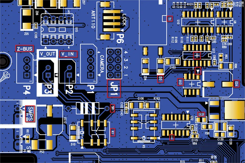
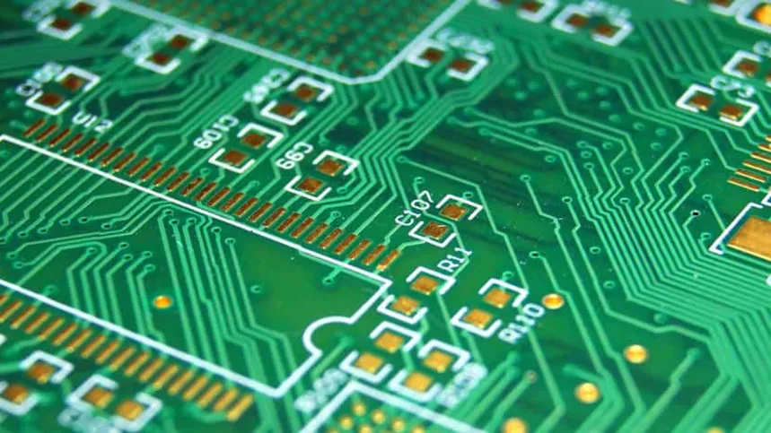
Silkscreen, also known as the legend or nomenclature layer, refers to the printed ink applied over the solder mask on a PCB's surface. It includes text, symbols, component identifiers, and graphical elements like logos, all designed to convey information and identity. Traditionally, silkscreen focused on functionality, such as polarity marks and reference designators, but its potential for PCB aesthetics has grown with advanced printing techniques. In branding contexts, silkscreen branding elements allow engineers to embed company logos, product names, or decorative patterns directly onto the board, creating a cohesive visual identity.
The relevance of silkscreen for branding stems from its permanence and visibility in end-user products. Unlike stickers or labels that may peel off, silkscreen withstands thermal cycling, solvents, and mechanical stress, ensuring long-term visual appeal. For electric engineers working on visible PCBs in enclosures or prototypes, this layer differentiates prototypes from production boards and reinforces brand loyalty. Moreover, high-quality silkscreen contributes to perceived product quality, influencing customer trust in sectors like medical devices and automotive electronics. Neglecting PCB aesthetics here can result in generic-looking boards that fail to leverage the full branding potential of the design.
Industry standards like IPC-4781 outline qualification requirements for legend inks, ensuring adhesion and legibility under operational stresses. This standard emphasizes testing for color fastness and resistance to environmental factors, directly supporting reliable silkscreen branding elements. By adhering to such guidelines, engineers balance creativity with manufacturability.
Technical Principles of Silkscreen Application
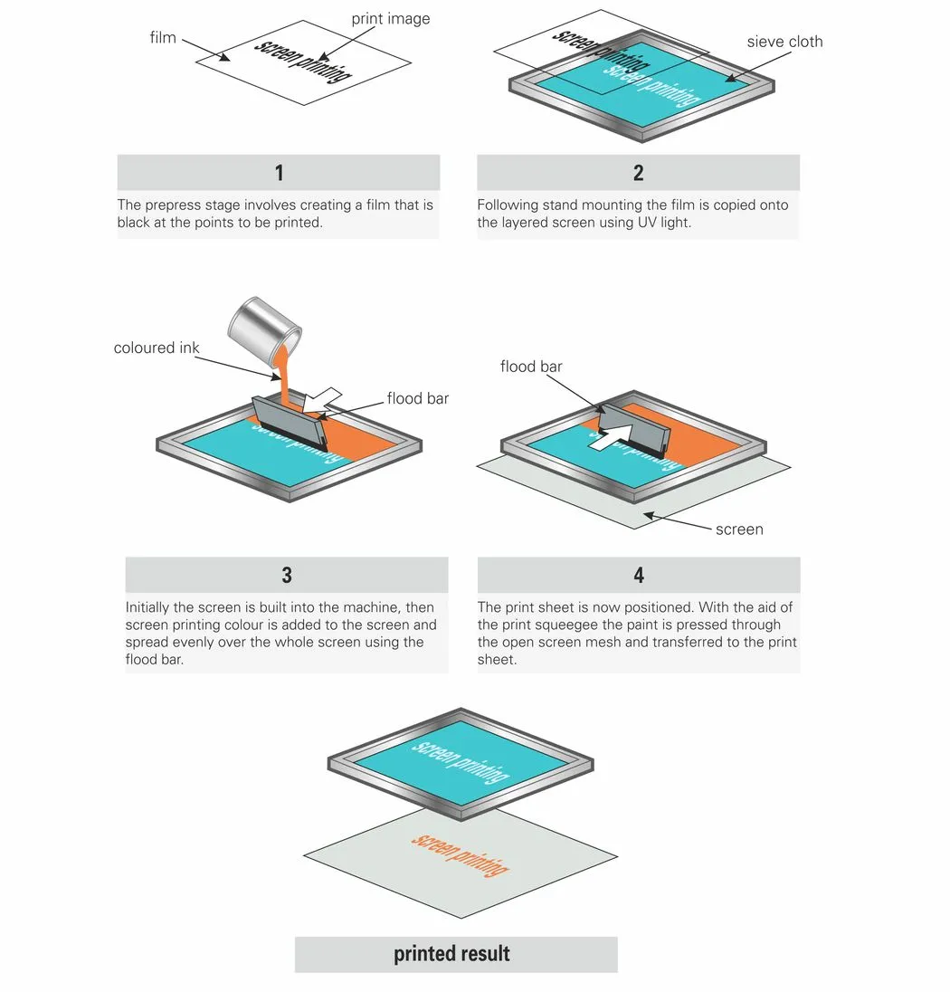
Silkscreen application begins after solder mask curing, using processes like traditional screen printing, liquid photoimageable (LPI) ink, or direct legend printing. In screen printing, a stencil stretched over a frame blocks ink except where openings allow it to transfer onto the PCB surface. The ink, typically epoxy-based, cures via UV exposure or thermal baking to form a durable layer approximately 20 to 30 microns thick. LPI methods offer higher resolution by applying liquid ink and exposing it through a photomask, ideal for intricate logos and fine text in silkscreen branding elements.
Key technical considerations include ink compatibility with the solder mask, as mismatches can lead to delamination during reflow. White ink remains the most common choice due to its high contrast against green or blue solder masks, optimizing PCB aesthetics. Engineers must account for registration accuracy, typically held to within 0.1 mm, to prevent misalignment over pads or traces. Curing profiles follow manufacturer specifications to achieve solvent resistance per IPC-A-600 acceptability criteria.
Environmental factors influence silkscreen durability, including humidity during printing and post-cure storage conditions. Standards mandate tests for adhesion via tape pull and scratch resistance, ensuring logos and visual appeal persist through assembly. Electric engineers benefit from understanding these principles to specify designs that manufacturers can reproduce consistently.
Best Practices for Silkscreen Branding Elements
Effective silkscreen design starts with vector-based artwork in EDA software, converting logos to monochrome outlines for optimal ink deposition. Maintain minimum line widths of at least 0.1 mm and character heights above 1 mm to ensure legibility across fabrication tolerances. Placement avoids solder pads, vias, and fiducials by at least 0.15 mm clearance, preventing ink bleed during reflow that could short circuits. For PCB aesthetics, position logos in non-critical areas like board edges or corners, using symmetry to enhance visual balance.
Color selection prioritizes contrast; white on dark solder masks excels, while black suits lighter masks for sharp logos and visual appeal. Limit to single-color printing for cost efficiency, reserving multi-color for high-end prototypes via advanced LPI. Test artwork at reduced scale to verify fill patterns in dense areas, avoiding moiré effects that degrade silkscreen branding elements. Incorporate version numbers or date codes alongside branding for traceability without cluttering aesthetics.
Orient all text unidirectionally for readability during inspection, aligning with assembly flow. Simulate solder mask coverage in design tools to predict final PCB aesthetics, iterating for maximum impact.
Integrating Logos and Visual Appeal in PCB Design
Logos demand scalable vector formats, simplifying complex shapes to bold lines that render crisply at small sizes. Engineers scale logos to 5 to 10 mm wide, ensuring details like text within them remain distinct post-printing. Integrate them into the silkscreen layer alongside functional markings, using negative space for emphasis. This approach amplifies visual appeal, making the PCB resemble a branded product component.
Consider board contour and layer stackup; top-side silkscreen suits most cases, with bottom-side reserved for dense top populations. For double-sided branding, mirror elements carefully to maintain cohesion. Visual simulations in 3D renderings help preview PCB aesthetics under various lighting, guiding refinements.
Advanced techniques like matte inks reduce glare for premium logos and visual appeal. Compliance with IPC-A-600 ensures markings withstand handling, preserving branding integrity.
Balancing Functionality with Aesthetic Branding
Silkscreen must not interfere with electrical performance or assembly yields. Avoid printing over test points or connectors, as ink buildup alters contact resistance. In high-density designs, prioritize reference designators over decorative elements, allocating space proportionally. Electric engineers evaluate trade-offs using design rule checks for silkscreen-to-feature spacing.
Thermal expansion differences between ink and substrate require robust adhesion testing per standards. Reflow profiles up to 260°C test ink integrity, with failures manifesting as cracking in logos. Proactive design reviews mitigate these, sustaining both PCB aesthetics and reliability.
Case Insights: Enhancing Brand in Complex Assemblies
In a hypothetical consumer router project, engineers incorporated a stylized logo via LPI silkscreen on the top layer, achieving crisp edges despite 0.08 mm lines. Placement near the edge maximized visibility post-assembly, boosting perceived quality. Challenges arose from green solder mask tinting white ink slightly yellow post-reflow, resolved by selecting UV-stable formulations. Yield improved 2% after optimizing clearances, demonstrating silkscreen branding elements' dual role in aesthetics and function.
Similar insights apply to industrial controllers, where etched-like effects via ink removal simulate premium finishes. These examples underscore structured approaches for electric engineers.
Conclusion
Silkscreen transforms PCBs from functional necessities into branded statements, leveraging PCB aesthetics through thoughtful logos and visual appeal. Electric engineers can harness silkscreen branding elements by following technical principles, best practices, and standards like IPC-4781 and IPC-A-600. This integration enhances product differentiation without sacrificing performance. Prioritize contrast, placement, and durability in designs to achieve professional results. Ultimately, mastering silkscreen elevates the entire electronics ecosystem, aligning engineering precision with marketing impact.
FAQs
Q1: How does silkscreen contribute to PCB aesthetics in engineering designs?
A1: Silkscreen adds logos and visual appeal directly on the board surface, contrasting with solder mask for striking effects. Engineers ensure high-resolution printing for crisp details, enhancing overall PCB aesthetics. Standards like IPC-A-600 guide legibility, balancing branding with functionality in electric designs. This layer persists through assembly, providing enduring visual identity.
Q2: What are key considerations for silkscreen branding elements on PCBs?
A2: Prioritize minimum line widths and clearances to avoid assembly issues while embedding logos effectively. Select inks for contrast and durability against reflow temperatures. Placement in non-functional areas maximizes PCB aesthetics without risking performance. Adherence to IPC guidelines ensures manufacturability. Electric engineers test prototypes for real-world appeal.
Q3: Can custom logos improve visual appeal in high-volume PCB production?
A3: Yes, vector-based logos scale reliably, integrating seamlessly into silkscreen layers for consistent branding. High-contrast choices elevate PCB aesthetics across panels. Processes like LPI support fine details in production runs. Engineers verify adhesion per standards to maintain logos post-assembly. This approach strengthens brand recognition in end products.
Q4: What standards govern silkscreen quality for branding on PCBs?
A4: IPC-4781 specifies ink qualification for adhesion and environmental resistance, crucial for durable logos. IPC-A-600 defines acceptability criteria for markings, ensuring legibility. These align silkscreen branding elements with industry reliability. Electric engineers reference them to optimize visual appeal and function. Compliance minimizes defects in production.
References
IPC-A-600K — Acceptability of Printed Boards. IPC, 2020
IPC-4781 — Qualification and Performance Specification for Permanent Legend Inks. IPC, 2008
IPC-6012E — Qualification and Performance Specification for Rigid Printed Boards. IPC, 2017


