ALLPCB


Introduction
Precision in PCB drilling plays a central role in maintaining signal integrity within high-speed electronic systems. Engineers working on advanced designs must consider how hole placement influences impedance characteristics and overall circuit performance. Small deviations in via or through-hole positioning can introduce discontinuities that affect signal propagation. This article examines the engineering considerations behind PCB drilling accuracy and its direct relationship to reliable high-speed operation. Structured approaches to design and manufacturing help address these factors effectively.
Why Hole Placement Accuracy Matters in High-Speed PCB Design
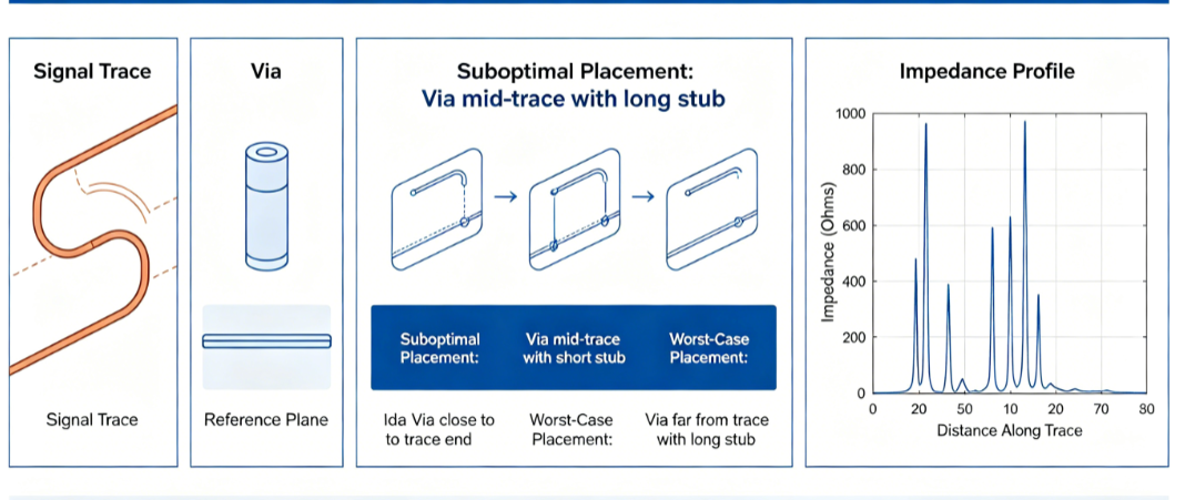
Hole placement tolerance directly affects the electrical behavior of vias and interconnects in multilayer boards. In high-speed PCB design, even minor offsets can alter the intended impedance profile along a signal path. This variation may lead to reflections or increased insertion loss, compromising data transmission quality. Designers therefore prioritize drilling accuracy to support consistent impedance matching across critical traces. The relationship between mechanical positioning and electrical performance becomes especially important as operating frequencies rise.
Proper positioning also helps control crosstalk between adjacent signals. When holes are located with greater precision, the return path remains more predictable, reducing unintended coupling. Manufacturing processes must align with design intent to achieve these outcomes consistently. Engineers evaluate placement requirements early in the layout phase to guide subsequent fabrication steps.
Technical Principles of PCB Drilling and Signal Integrity
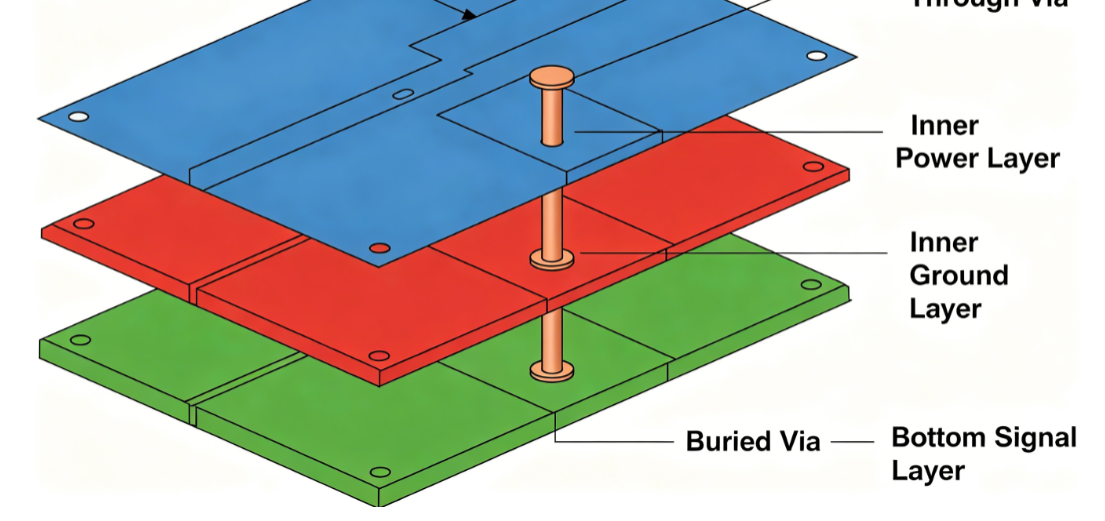
Drilling creates the vertical interconnects essential for connecting layers in a printed circuit board. The accuracy of these holes determines how closely the actual via structure matches the modeled geometry used for impedance calculations. Deviations in position or diameter can change the capacitance and inductance associated with each via. In high-speed applications, these changes manifest as impedance mismatches that distort waveforms. Structured analysis of via parasitics forms a key part of the design process.
Signal integrity depends on maintaining controlled impedance throughout the transmission path. Hole placement influences the reference plane proximity and the overall loop inductance. When placement tolerances are managed carefully, the via behaves more like an extension of the trace rather than a disruptive element. Engineers apply simulation tools to predict these effects before committing to fabrication. This proactive evaluation supports decisions on stack-up and via configuration.
The drilling process itself involves mechanical or laser methods, each with distinct characteristics regarding positioning repeatability. Mechanical drilling offers robustness for larger holes, while laser techniques provide finer control for microvias. Regardless of method, the final placement must satisfy both mechanical and electrical requirements. Alignment between design files and manufacturing equipment determines the achievable accuracy.
Best Practices for Achieving PCB Drilling Accuracy
Design rules should incorporate sufficient margins for hole placement based on the capabilities of the fabrication process. Specifying appropriate pad sizes and clearances around vias helps accommodate typical positioning variations. Engineers often review stack-up details and via aspect ratios to ensure manufacturability alongside electrical performance goals. Collaboration between design and manufacturing teams clarifies expectations for hole location tolerances.
Process controls during drilling, such as registration techniques and panel fixturing, contribute to consistent results. Post-drill inspection verifies that actual positions align with design specifications. When discrepancies arise, adjustments to artwork or compensation in the drill program can be applied. These steps help preserve the intended impedance characteristics in the finished board.
Material selection and panel handling also influence drilling outcomes. Warpage or dimensional changes in the substrate can affect hole positioning relative to copper features. Designers account for these variables by applying appropriate design for manufacturability guidelines. Regular communication with fabricators ensures that specified requirements remain achievable.
Quality Considerations and Industry Standards
Adherence to established industry standards provides a framework for defining acceptable hole quality and placement. IPC-6012E outlines qualification and performance requirements for rigid printed boards, including aspects relevant to via structures. This standard helps establish consistent criteria across different production environments.
Inspection criteria further support verification of drilling results. IPC-A-600K supplies visual and dimensional acceptance guidelines that complement performance specifications. Application of these references assists engineers in evaluating whether fabricated boards meet the needs of high-speed designs.
Design guidelines in IPC-2221 address general considerations for printed board layouts, including via placement relative to signal integrity. Integrating these principles early in the development cycle supports both electrical performance and manufacturing reliability.
Conclusion
Precise PCB drilling supports optimal signal integrity by minimizing impedance variations and maintaining predictable via behavior. Engineers achieve better outcomes through careful attention to placement tolerances, design rules, and manufacturing alignment. Reference to recognized standards such as IPC-6012E, IPC-A-600K, and IPC-2221 provides a consistent basis for requirements and verification. Structured application of these practices helps ensure reliable performance in high-speed PCB designs.
FAQs
Q1: How does PCB drilling accuracy influence signal integrity in high-speed designs?
A1: PCB drilling accuracy affects via positioning, which in turn impacts impedance continuity along signal paths. Consistent hole placement supports better impedance matching and reduces reflections that can degrade high-frequency performance. Engineers evaluate these factors during layout to maintain overall signal quality.
Q2: What role does hole placement tolerance play in impedance matching?
A2: Hole placement tolerance determines how closely actual via geometry matches the modeled parameters used for impedance calculations. Controlled tolerances help preserve the target impedance profile and minimize discontinuities. This consideration becomes critical in high-speed PCB design where small variations produce measurable effects.
Q3: Why is precision drilling important for high-speed PCB applications?
A3: Precision drilling ensures that interconnect structures do not introduce excessive parasitics or impedance mismatches. Accurate hole locations contribute to stable signal propagation and reduced crosstalk. These attributes support reliable operation at elevated data rates.
Q4: How do industry standards guide PCB drilling requirements?
A4: Standards such as IPC-6012E establish performance expectations for via structures and board qualification. Complementary documents like IPC-A-600K provide criteria for evaluating fabricated features. Designers reference these to align manufacturing outputs with electrical objectives.
References
IPC-6012E — Qualification and Performance Specification for Rigid Printed Boards. IPC, 2017
IPC-A-600K — Acceptability of Printed Boards. IPC, 2020
IPC-2221 — Generic Standard on Printed Board Design. IPC, 2012