 ALLPCB


Introduction
Printed circuit board inspection plays a central role in ensuring that assembled electronics meet performance and reliability expectations across industries. Engineers and quality teams rely on established criteria to evaluate soldering quality, component placement, and overall board condition during production and incoming inspection. These criteria help distinguish acceptable units from those that require rework or rejection, reducing field failures and supporting consistent manufacturing output. For electric engineers working on complex designs, understanding these standards provides a common language for communicating requirements with fabrication and assembly partners. Clear inspection guidelines also support traceability and documentation practices that align with broader quality management systems.
What Is IPC-A-610 PCB Inspection and Why It Matters
IPC-A-610 PCB inspection defines visual acceptance criteria for electronic assemblies, covering solder joints, component orientation, and board surface conditions. The standard organizes requirements into three product classes that reflect increasing levels of performance and reliability demands. Class 1 addresses general electronic products where the primary concern is basic functionality, while Class 2 covers dedicated service electronics that require extended operation. Class 3 applies to high-performance equipment where downtime cannot be tolerated and long-term reliability is essential. These classifications allow teams to select inspection thresholds that match the end-use environment without imposing unnecessary stringency on every assembly.
Related Reading: The Ultimate Checklist for IPC A 610 Visual Inspection: Component Placement
Technical Principles of PCB Acceptance Criteria
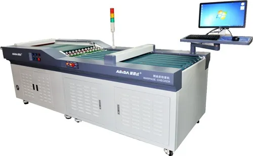
Acceptance decisions rest on measurable attributes such as solder fillet height, wetting angle, and lead protrusion through plated holes. Engineers examine each joint for complete coverage, absence of cracks, and proper fillet shape that indicates adequate thermal and mechanical bonding. Component placement must maintain specified clearances to prevent bridging or short circuits, and lead forming must avoid excessive stress on terminations. Board-level conditions such as warpage, delamination, or contamination are evaluated against limits that preserve electrical performance and mechanical integrity during subsequent handling and operation.
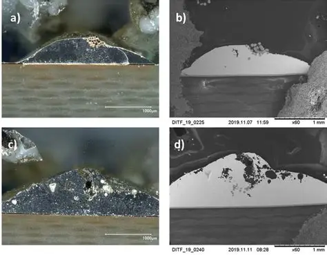
Practical Solutions and Best Practices for PCB Quality Standards
Effective implementation begins with documented inspection procedures that specify lighting, magnification, and viewing angles for each feature. Operators follow a systematic sequence that checks board edges first, then proceeds to component rows and finally to individual solder connections. When discrepancies appear, teams compare them against illustrated examples in the standard to determine the appropriate class and disposition. Calibration of inspection tools and regular training sessions maintain consistency across shifts and facilities. Documentation of inspection results supports root-cause analysis when process adjustments become necessary.
Related Reading: Automated Optical Inspection (AOI) for Conformal Coating: Ensuring IPC-A-610 Compliance
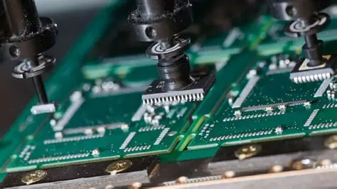
Factory-Driven Insights on IPC Standards for PCB
Production environments apply these criteria at multiple stages, from first-article verification through ongoing sampling and final audit. Process engineers correlate inspection findings with reflow profiles and placement accuracy data to identify upstream variables that influence acceptance rates. When assemblies consistently meet Class 2 or Class 3 requirements, yield improvements and reduced rework follow naturally. Teams also use the standard to define incoming inspection protocols for purchased boards and components, ensuring that quality expectations remain aligned throughout the supply chain.
Conclusion
IPC-A-610 PCB inspection and related standards provide a structured framework that supports reliable evaluation of electronic assemblies. By aligning inspection practices with defined acceptance criteria, engineering and manufacturing teams achieve consistent quality outcomes while meeting the performance expectations of their specific product classes. Continued attention to these guidelines helps maintain traceability and supports ongoing process refinement in demanding production settings.
FAQs
Q1: What does IPC-A-610 PCB inspection cover in terms of acceptance criteria?
A1: IPC-A-610 PCB inspection establishes visual and dimensional requirements for solder joints, component mounting, and board condition. It defines three product classes that guide the level of scrutiny applied during manufacturing and incoming checks. Engineers use these criteria to decide whether an assembly meets the reliability needs of its intended application.
Q2: How do PCB acceptance criteria help electric engineers during design review?
A2: PCB acceptance criteria translate end-use reliability goals into measurable inspection limits that can be reviewed before production begins. Electric engineers reference these limits when specifying component footprints, solder mask clearances, and board flatness requirements. This alignment reduces the likelihood of design features that would consistently fall outside acceptable ranges.
Q3: Why are IPC standards for PCB important in high-volume manufacturing?
A3: IPC standards for PCB supply a common set of acceptance rules that production teams can apply uniformly across multiple lines and suppliers. Consistent application supports predictable yields and simplifies communication when quality issues arise. The standards also provide illustrated examples that help operators make repeatable judgments without relying on subjective interpretation.
Q4: What role does board warpage play in PCB quality standards evaluation?
A4: Board warpage is assessed against limits that ensure components remain properly seated and solder joints form without excessive stress. Excessive distortion can lead to open circuits or cracked terminations after reflow or during thermal cycling. Inspection procedures therefore include checks for flatness as part of overall acceptance under applicable quality standards.





