ALLPCB


Smart grid systems rely on advanced electronics to manage power distribution, integrate renewable sources, and enable real-time monitoring. Printed circuit boards serve as the foundation for these functions, and their assembly directly affects long-term reliability in demanding electrical environments.
Engineers must select assembly methods that accommodate high-power components, thermal stresses, and vibration while maintaining signal integrity. Effective techniques balance density, mechanical strength, and inspection rigor to meet operational demands.
Why Precise PCB Assembly Matters for Smart Grid Applications
Smart grid infrastructure operates under continuous electrical loads, temperature fluctuations, and potential electromagnetic interference. Assembly quality influences everything from fault detection accuracy to system uptime. Poor soldering or component placement can lead to intermittent failures that compromise grid stability. Practical assembly choices therefore prioritize durability alongside performance to support safe and efficient power management.
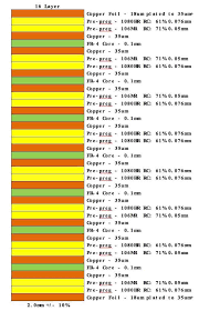
SMT Assembly for Smart Grid PCBs
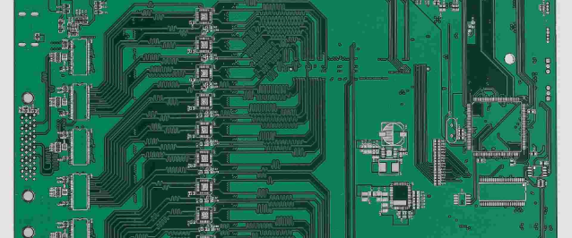
Surface mount technology places components directly onto the board surface, enabling compact layouts suitable for control modules and sensor interfaces. This approach supports high component density while reducing overall board size, which benefits space-constrained substation equipment. Engineers often apply SMT where fine-pitch devices handle data processing tasks. Process control during reflow soldering remains essential to avoid defects such as tombstoning or insufficient wetting on pads exposed to power surges.
Troubleshooting common SMT issues involves verifying paste volume and reflow profiles against board thermal mass. Variations in copper distribution can create uneven heating, requiring profile adjustments based on thermocouple measurements. Consistent stencil design and placement accuracy help maintain joint integrity across production batches.
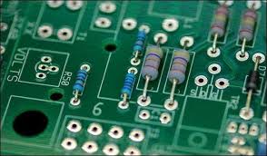
Through-Hole Assembly for Smart Grid PCBs
Through-hole technology inserts component leads into drilled holes and solders them on the opposite side, providing strong mechanical bonds ideal for high-current connectors, transformers, and power semiconductors. These joints withstand greater mechanical stress and thermal cycling compared with surface-only attachments. Smart grid designs frequently combine through-hole parts for power paths with surface-mounted devices for logic functions.
Wave soldering or selective soldering processes require careful masking of nearby SMT areas to prevent damage. Engineers monitor hole fill percentages and fillet formation to ensure electrical continuity under load. Vibration testing often reveals weaknesses in through-hole joints, prompting reinforcement techniques such as clinching leads before soldering.
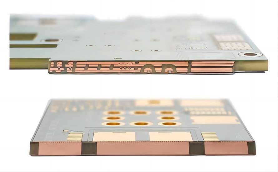
Mixed Technology Assembly for Smart Grid PCBs
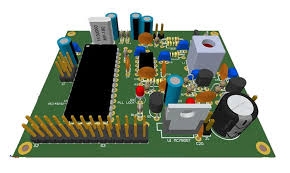
Many smart grid boards integrate both surface mount and through-hole components to optimize electrical and mechanical performance. Mixed assembly sequences typically begin with SMT placement and reflow, followed by through-hole insertion and secondary soldering. This order minimizes thermal exposure to temperature-sensitive surface devices while securing robust power connections.
Process planning addresses potential warpage from differing material expansions during multiple heating cycles. Fixture design and support pins help maintain flatness, reducing stress on fine-pitch joints. Engineers evaluate solder mask and surface finish compatibility to prevent bridging between technologies during final assembly.
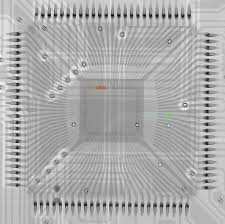
Inspection Methods: AOI and X-ray for Smart Grid PCB Assembly
Automated optical inspection scans board surfaces for visible defects such as misaligned components, insufficient solder, or bridging. High-resolution cameras compare actual images against programmed criteria, flagging issues early in the production flow. AOI proves effective for top-side SMT joints but cannot evaluate hidden connections beneath components.
X-ray inspection complements AOI by revealing internal joint quality, including voids in ball grid arrays or barrel fill in through-hole connections. This method detects issues invisible to optical systems, particularly important for power modules where incomplete wetting could cause overheating. Combined inspection strategies improve overall defect detection rates while supporting traceability requirements.
Best Practices and Troubleshooting Guidance
Engineers begin with design for manufacturability reviews that align component selection with chosen assembly processes. Thermal profiling tailored to board construction prevents damage during reflow or wave soldering. Regular calibration of placement equipment and inspection systems maintains consistency across runs.
When defects appear, root cause analysis examines paste rheology, placement force, and reflow atmosphere. For mixed boards, sequencing adjustments often resolve bridging or insufficient hole fill. Documentation of process parameters supports continuous improvement and compliance with established quality frameworks.
Industry standards such as IPC-A-610 guide acceptability criteria for electronic assemblies, helping teams define clear pass-fail thresholds. J-STD-001 outlines soldering requirements that apply across surface mount, through-hole, and mixed configurations.
Conclusion
Smart grid reliability depends on assembly techniques that deliver both electrical performance and mechanical robustness. SMT, through-hole, and mixed approaches each address specific design needs when executed with appropriate process controls. Thorough inspection using AOI and X-ray methods catches defects before they reach the field. Adhering to recognized standards throughout production supports consistent quality and long service life in critical power applications.
FAQs
Q1: What considerations guide SMT assembly for smart grid PCBs?
A1: SMT assembly for smart grid PCBs focuses on achieving high component density while managing thermal profiles during reflow. Engineers verify paste deposition and placement accuracy to prevent defects under electrical and environmental stress. Process adjustments account for copper distribution and board warpage to maintain joint reliability in power control modules.
Q2: How does through-hole assembly for smart grid PCBs differ from surface mount methods?
A2: Through-hole assembly for smart grid PCBs provides stronger mechanical attachment for high-current components exposed to vibration and thermal cycling. Leads inserted through the board create robust connections that complement surface-mounted devices used for signal processing. Selective soldering techniques help protect nearby SMT areas during the secondary process.
Q3: When is mixed technology assembly for smart grid PCBs the preferred approach?
A3: Mixed technology assembly for smart grid PCBs combines surface mount density with through-hole strength for boards handling both power and control functions. Proper sequencing of SMT reflow before through-hole soldering minimizes thermal damage while ensuring mechanical integrity. Fixture support during processing reduces warpage that could affect fine-pitch joints.
Q4: Why use automated optical inspection (AOI) and X-ray inspection for smart grid PCB assembly?
A4: Automated optical inspection (AOI) for smart grid PCBs detects visible placement and soldering issues on accessible surfaces early in production. X-ray inspection for smart grid PCB assembly reveals hidden joint quality such as voids or incomplete fills in power components. Together these methods support comprehensive quality verification aligned with industry expectations.
References
IPC-A-610G — Acceptability of Electronic Assemblies. IPC, 2017
J-STD-001H — Requirements for Soldered Electrical and Electronic Assemblies. IPC, 2020
IPC-6012E — Qualification and Performance Specification for Rigid Printed Boards. IPC, 2017
ISO 9001:2015 — Quality Management Systems. ISO, 2015