ALLPCB


Introduction
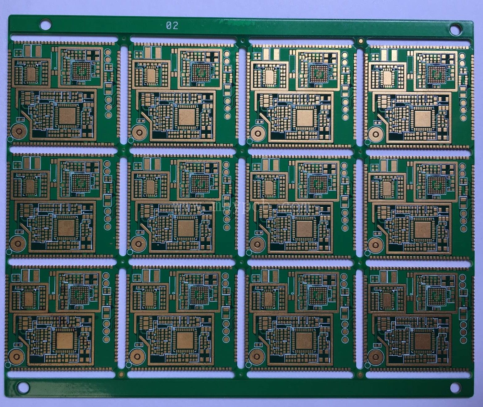
Panelization remains a cornerstone of efficient PCB manufacturing, allowing multiple boards to be produced on a single panel to cut costs and streamline assembly processes. However, improper panelization can introduce significant PCB panelization warpage, leading to challenges in soldering, component placement, and overall yield. Electrical engineers must prioritize strategies that maintain board flatness throughout fabrication and assembly. This article explores proven panelization techniques, focusing on array design, v-score impact, and breakaway tabs to minimize warpage. By aligning designs with manufacturing realities, teams can achieve higher reliability and reduce defects. Factory insights reveal that thoughtful panel layouts directly correlate with improved process control.
Understanding PCB Warpage and Its Relevance in Panelized Production
PCB warpage manifests as bowing or twisting, where the board deviates from flatness due to internal stresses. In panelized formats, these distortions amplify because stresses propagate across interconnected boards during thermal cycling. Industry standards like IPC-6012 outline acceptability criteria for bow and twist, emphasizing the need for flatness in surface-mount applications. Warpage exceeds limits when panels undergo lamination, drilling, plating, or reflow, compromising pick-and-place accuracy and solder joint integrity. For electrical engineers, understanding this interplay is crucial, as even minor deformations can cause open circuits or bridging in high-density assemblies. Panelization, while economical, demands precision to preserve dimensional stability.
Primary Causes of Warpage in Panelized PCBs
Asymmetric copper distribution across the panel creates uneven thermal expansion during reflow, pulling boards into curvature. Large panel sizes exacerbate this by increasing overall rigidity demands, leading to higher stress concentrations at edges. V-scoring and tab connections introduce localized strains if not optimized, as cutting processes alter material properties near separation lines. Moisture absorption prior to processing further aggravates warpage through vaporization in ovens. Inadequate support during handling or assembly allows gravitational forces to compound thermal effects. Factory experience shows that neglecting these factors results in up to doubled rejection rates in assembly lines.
Array Design Principles to Combat PCB Panelization Warpage
Effective array design starts with symmetry, arranging boards in mirrored or rotated patterns to balance copper density and material thickness. Electrical engineers should aim for even distribution of feature-heavy and sparse areas across the panel, preventing one-sided expansion. Rotating individual boards by 90 or 180 degrees within the array can equalize stress vectors, a technique proven in high-volume production. Limit panel dimensions to standard working sizes, avoiding oversized layouts that amplify flexure. Incorporate fiducial marks symmetrically for alignment, ensuring consistent handling. These array design practices distribute loads uniformly, directly reducing PCB panelization warpage.
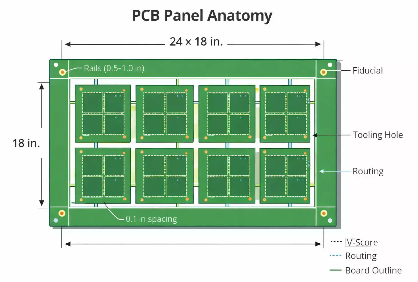
Orienting boards with consistent grain direction relative to the panel frame maintains laminate integrity. Thicker carrier rails around the perimeter add stiffness without adding cost. Testing prototypes in simulated reflow conditions validates array efficacy early. Collaboration between design and fabrication teams refines these layouts iteratively.
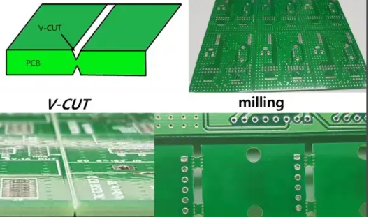
Addressing V-Score Impact on Panel Integrity
V-scoring provides clean, straight-line separation but poses risks to warpage if depth or angle is mismatched to board thickness. Typically executed from both sides to about one-third depth each, improper v-grooves concentrate stresses, cracking during depaneling or inducing bow. Engineers must specify angles between 30 and 45 degrees to distribute shear forces evenly, minimizing microcracks. Maintain generous keep-out zones, at least several millimeters from components or traces, to avoid vibration transmission during scoring. V-score impact heightens in thin boards or those with heavy copper, where groove proximity alters local CTE behavior. Factory-driven adjustments, like staged scoring passes, mitigate these effects effectively.
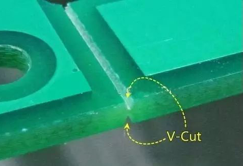
Hybrid approaches, combining v-scores with jump scoring over rails, prevent full cuts that weaken panels prematurely. Post-scoring inspections verify groove uniformity, catching deviations early. Align v-scores parallel to board edges for predictable stress paths.
Optimizing Breakaway Tabs for Warpage Reduction
Breakaway tabs, often with perforated mouse bites, offer flexible depaneling while reinforcing panel stability during processing. Strategic placement along all edges, spaced evenly, counters twisting by providing uniform support. Tab width and length should scale with board size, typically wider for larger arrays to resist flex. Perforation patterns, such as staggered holes, facilitate clean snaps without residual stress that propagates warpage. Electrical engineers benefit from tabs positioned away from critical traces, reducing delamination risks post-separation. This method excels in irregular shapes where v-scoring falters.
Thicker tabs enhance rigidity, particularly for multilayer boards prone to thermal deflection. Combine with routing for curved edges, ensuring tabs bridge straight segments only. Deburring fixtures post-depaneling preserve edge quality, avoiding secondary warpage from handling damage.
Additional Manufacturing Best Practices
Pre-baking panels removes moisture, stabilizing dimensions before lamination or assembly. Controlled cooling rates post-reflow prevent rapid contraction gradients. Support fixtures during soldering maintain flatness under heat. Material selection with matched CTE layers complements panelization efforts. J-STD-020 guidelines for handling sensitivity underscore baking protocols. Integrating these with panel strategies yields robust outcomes.
Conclusion
Mastering panelization strategies transforms potential warpage pitfalls into manufacturing strengths. Symmetric array design, careful v-score management, and robust breakaway tabs form the triad for minimizing PCB panelization warpage. Electrical engineers armed with these factory-aligned practices ensure compliance with standards like IPC-6012, boosting yield and reliability. Proactive design reviews and process validation pay dividends in high-volume runs. Prioritizing flatness from panel inception leads to seamless assembly and enduring performance.
FAQs
Q1: What role does array design play in PCB panelization warpage?
A1: Array design influences PCB panelization warpage by balancing thermal and mechanical stresses across the panel. Symmetric layouts with mirrored or rotated boards equalize copper distribution, reducing uneven expansion during reflow. Factory standards recommend limiting board count and incorporating rails for stiffness. This approach aligns with manufacturing tolerances, preventing bow in assembled panels. Proper fiducials aid precise handling.
Q2: How does v-score impact affect PCB flatness?
A2: V-score impact arises from stress concentrations at groove lines, potentially inducing warpage if depth exceeds one-third board thickness per side. Optimal angles of 30 to 45 degrees distribute forces evenly, minimizing cracks. Keep-out zones protect components from vibration. Engineers should verify groove uniformity post-processing to maintain panel integrity throughout assembly.
Q3: Why are breakaway tabs essential in warpage reduction?
A3: Breakaway tabs provide structural reinforcement during fabrication, countering flexure in panelized arrays. Perforated designs with mouse bites enable stress-free depaneling, avoiding residual distortions. Even spacing and adequate width scale with panel size for optimal support. This method suits complex shapes, preserving flatness better than pure routing in many cases.
Q4: What standards guide panelization for warpage control?
A4: IPC-6012 specifies bow and twist criteria for rigid boards, guiding panelization to meet assembly needs. J-STD-020 addresses moisture effects that exacerbate warpage in panels. These ensure designs withstand thermal cycling without deformation.